Introduction
The modern world is vertically integrated on the transistor. A single leading-edge chip contains tens of billions of these tiny electronic switches, connected by roughly 60 miles of wiring – all in a form factor the size of a quarter.[1] The incredible technology trajectory of the integrated circuit (IC), from individual transistors soldered together by hand to the precise layering of billions of transistors at the nanoscale, has made possible technologies like personal computers, GPS, the Internet, and smartphones.[2] The power of these technologies are a testament to the exponential gains in compute attained over the past 75 years: an average iPhone contains more processing power than the entirety of the National Aeronautics and Space Administration (NASA) at the time of the Apollo 11 moon landing.[3]
Today, however, the fundamental processes that have enabled decades of progress in microelectronics are breaking down. Moore’s Law scaling has slowed and is projected to reach its limits within the next 15 years.[4] This trend has profound implications for the global economy and national defense:[5] continued technological progress in fields ranging from AI to biotechnology to materials science depends on the regular doublings in compute predicted by Moore’s Law.[6] The United States has long benefitted from its position as the global driver of innovation in advanced compute[7] and microelectronics, but continued leadership is not assured.
Compute and microelectronics consist of layers of enabling technologies. Taken together, these layers can be conceptualized as a single technology stack. The compute stack starts with materials: roughly half the elements in the periodic table have been used previously to build microelectronics.[8] Devices are tiny switches which correspond to 0s and 1s in digital computing. Circuitsstring devices together to perform compute functions. Architectures string components together to create a coherent, large-scale computing system. Algorithmsare sequences of instructions that the computer uses to solve a problem. The top layer, software, is the collection of instructions and programs that tell the computer what to do, while the applications layer serves as a bridge to solve real-world problems. Lower layers are supported by process innovation – new methods for how to build chips – and tools used to both design and manufacture them.
Ultimately, moving beyond Moore’s Law will require upgrading individual layers of the stack while testing fundamental assumptions about how computation takes place. Such a task demands a national effort to build, scale, and integrate emerging compute paradigms that employ novel materials, specialized hardware, and next-generation manufacturing techniques. Setting national ambitions for compute will drive progress in microelectronics and beyond. The nation that can successfully develop and deploy post-Moore’s Law compute paradigms at scale will gain the inside track during an era where computing power and AI capabilities underpin scientific and technological progress across all other fields.
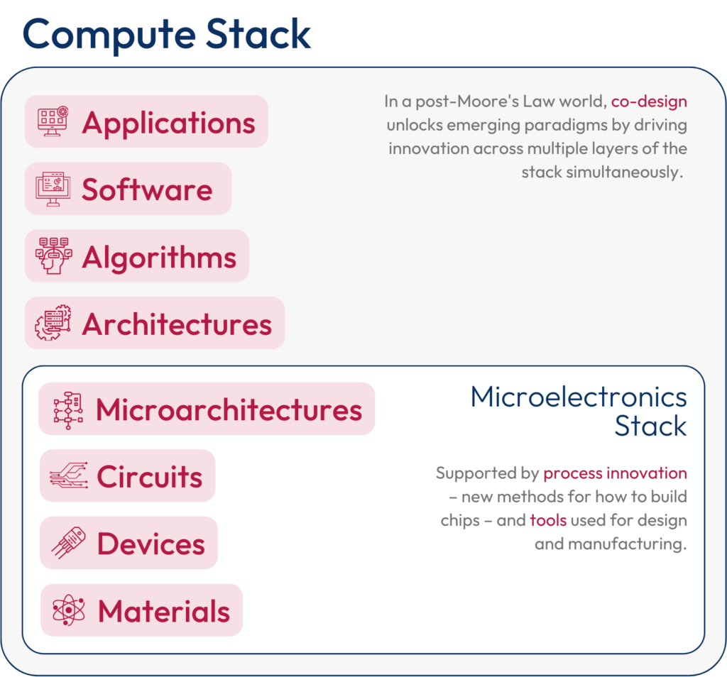
Graphic Source.[9]
Many roadmaps detail the possible vectors for the future of compute and microelectronics.[10] Yet the current moment demands a concrete plan to ensure the nation is positioned and organized for leadership in the post-Moore’s Law era. This document does not directly address the need to build additional fabrication facilities or implement “protect” measures such as export controls (see Appendix A). Instead, it provides a forward-looking, technology-focused strategy for how academia, the private sector, and government can collaborate to ensure U.S. and global democratic leadership in this critical technology through 2030 and beyond. In doing so, it draws from the strategic logic of the Positioning School.[11] As SCSP writes in Harnessing the New Geometry of Innovation, “winning strategies take the form of dominant positions in the relevant competition…at the national level, the American democracy often secures strategic technology positions by national endeavors that translate latent power into active power.”[12] In the same way that the Apollo Program galvanized the nation to win the space race, bold national technology goals can propel the entire American innovation ecosystem into positions of national advantage.
Desired Endstate
The United States dominates the post-Moore’s Law future by bringing the world into the era of heterogeneous integration, scaling breakthroughs across the compute stack, and establishing positions of advantage in new forms of computing.
We envision a world where:
- Emerging compute paradigms are scaled and combined, enabling a step-change in AI performance;
- The United States drives advances in heterogeneous integration and advanced packaging which allow for continued scaling in computing power, at a rate that approximates Moore’s Law;
- Novel compute paradigms and microelectronics breakthroughs are developed and scaled which drastically reduce the energy demand associated with computation;
- The innovation pipeline for modeling and scaling emerging post-complementary metal-oxide-semiconductor (CMOS) devices and materials becomes more robust;
- AI-enabled design tools become widely diffused and are used to develop new forms of computing, significantly reducing barriers to entry;
- The United States, with its allies and partners, addresses hardware security risks with policy moves and technology solutions while countering Beijing’s efforts to disrupt the global chip industry, minimizing impacts on critical infrastructure and U.S. and allied firms;
- Technology breakthroughs significantly reduce the cost of microelectronics fabrication. Such breakthroughs could begin to reverse industry concentration and would be in the interest of the United States and its allies and partners.
Central Policy
Chart a post-Moore’s Law future by catalyzing disruptive innovation via compute moonshots and build a flourishing atoms-to-architectures innovation pipeline that can develop, scale, and integrate novel materials and devices.[13] In parallel, make key supporting moves to address enabling factors that make future U.S. and democratic leadership possible.
Background
American inventors Jack Kilby and Robert Noyce separately invented the integrated circuit over the span of a few months between 1958 and 1959.[14] Their designs took transistors – tiny switches corresponding to the 0s and 1s that power digital computers – and pieced them together on a small, flat semiconductor “chip.” In 1965, Intel co-founder Gordon Moore made a monumental prediction about the trajectory of the technology, which later became known as Moore’s Law. Moore observed that the number of transistors on a chip was doubling regularly, and he projected this trend would continue for the foreseeable future.[15] For the next 55 years, the development of microelectronics and corresponding increases in computing power followed the trajectory of Moore’s Law.[16]
Today, however, the trajectory of Moore’s Law is uncertain as transistor “scaling” bumps up against the limits of physics.[17] Transistor scaling already hit its first insurmountable obstacle in the early 2000s, when transistors shrank to such a degree that it became impossible to process information faster without overheating the chip.[18] In response, firms rolled out multi-core processing units that performed many computations in parallel.[19] This innovation, sometimes called parallel computing, allowed industry to keep pace with Moore’s Law in terms of performance – and helped power the deep learning revolution in AI over the past decade.[20] But parallel computing also decoupled the long-established link between Moore’s Law scaling and gains in energy efficiency.[21] Energy demand from compute has steadily grown to the point that it now consumes an estimated five percent of the world’s generated electricity.[22]
Beyond energy challenges, driving transistors smaller and smaller has resulted in new levels of complexity, squeezing firms on both technology and economics.[23] Pushing deep into the nanoscale has come with a price tag: since the world’s first 3D transistor debuted in 2011, research and development (R&D) costs have risen by roughly a factor of ten.[24] In the coming years, designing a 2 nanometer (nm) chip is projected to cost an estimated $725 million.[25] Building a chip fab for 2nm chips, meanwhile, could cost upwards of $30 billion.[26] With costs showing no signs of slowing down, something has to give.
Geopolitical Context
For decades, the People’s Republic of China (PRC) has set its sights on building a domestic microelectronics industry. China’s chip industry has received over $200 billion in government support over the past two decades as a prime target in Beijing’s push for “indigenous innovation.”[27] Though the industry as a whole is still emerging (China has imported more semiconductors by value than any other product, including oil, for several years in a row),[28] individual firms have begun to break through, with several launching internationally competitive products.[29] China’s microelectronics industry benefits from access to virtually unlimited resources, a massive (and protected) domestic market, a growing and highly motivated pool of scientists and engineers, and an industrial espionage strategy with global reach.[30] Counting it out would be a mistake.
Graphic Source.[31]
Over the past five years, U.S. policymakers have recognized the geopolitical importance of microelectronics and their position as a key technology battleground.[32] The Trump Administration imposed export controls on certain high-end chips to PRC-champion Huawei and blocked Beijing’s attempts to acquire U.S.-headquartered chip firms Qualcomm and Micron.[33] In 2022, U.S. policy efforts reached a new peak with passage of the CHIPS & Science Act, landmark legislation which included $39 billion in manufacturing incentives across the microelectronics value chain and $11 billion for microelectronics R&D. The R&D program included funding for a National Semiconductor Technology Center (NSTC) to serve as a national innovation hub for the microelectronics ecosystem, as well as a National Advanced Packaging Manufacturing Program (NAPMP).[34] The Biden Administration also placed export controls on advanced chips for AI training and semiconductor manufacturing equipment, dealing a blow to Beijing’s microelectronics industry.[35]
Despite these efforts, risk vectors stemming from microelectronics still pose a threat to the national security and economic competitiveness of the United States and its allies and partners. PRC semiconductor producers are planning a massive buildout for lagging-edge chip nodes over the next five years, increasing their capacity by nearly as much as the rest of the world combined.[36] This buildout poses severe challenges not only for the competitiveness of U.S. and allied firms, but also for information security and privacy. Currently, there are few restrictions to block or screen these chips, which may contain vulnerabilities and backdoors, from being deployed in critical infrastructure sectors.[37]
In the coming years, cybersecurity at the hardware layer is likely to emerge as a key challenge due to the efforts of both nation-state and nonstate actors.[38] A range of mechanisms have emerged that allow malicious actors to insert vulnerabilities – which could function either as an “on-off switch” or as a backdoor for data exfiltration – directly into a chip’s hardware or firmware. In addition, side-channel and fault-injection attacks allow for chips to be targeted in the field.[39] These attacks typically cannot be patched immediately like software vulnerabilities. Technology trends towards heterogeneous integration (see below), where multiple “chiplets” from a range of third-party designers and foundries are combined to form a single system-in-package, will exacerbate these risks.[40]
Science & Engineering Beyond Moore’s Law
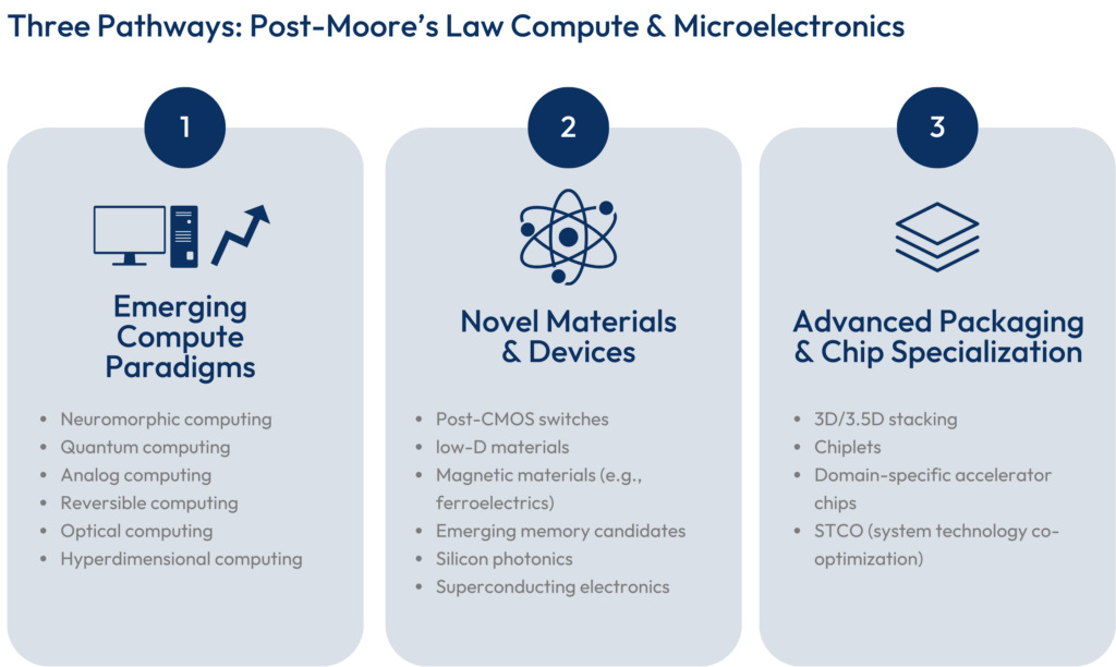
Ultimately, there are three fundamental pathways to innovating beyond transistor scaling.[41] The first approach involves a combination of 3D heterogeneous integration and specialized chip architectures. The former owes inspiration to Gordon Moore himself. In his seminal 1965 paper, Moore proposed that, instead of continuing to shrink transistors and cram them onto flat silicon wafers, continuing performance gains would require scaling chips vertically.[42] Today, this approach involves combining and connecting components vertically to form complex 3D microsystems.[43] The latter prong of this approach involves building specialized “accelerator” chips for particular applications, as these offer efficiencies and performance gains over their general-purpose counterparts. While these approaches offer a clear next step for microelectronics, they are subject to significant challenges and should not be the only approach the nation relies on.[44]
Second, novel materials and devices add new functionalities to key layers of the computing stack. A range of materials are emerging that promise significant improvements in energy efficiency. Novel post-CMOS device candidates are also emerging which harness different state variables – beyond the flow of electrons in traditional electronics – to perform calculations and store data. Photonics, for example, harnesses the power of light to transmit data from place to place,[45] while spintronics and ferroelectrics use unique properties of magnetic fields and electron spin to perform computation. Advances in these fields are essential and will be necessary to continue transistor scaling beyond 2030.
In the long run, supplying ever-increasing compute demand will require revolutionary, not evolutionary, advances in post-Moore’s Law paradigms.[46] Novel compute paradigms are emerging that require us to fundamentally reimagine how computation takes place.[47] To take one example, neuromorphic computing unlocks a new approach to compute based on the neural architecture of the human brain, allowing chips to operate at ultra-low power and potentially enabling new approaches to AI. Quantum computing, meanwhile, harnesses the power of the atom as a processor to solve problems that classical computers cannot. These new paradigms are typically built on novel hardware combinations and often require the creation of an entirely new software stack, but offer the greatest long-term promise to drive continued compute scaling. As such, they are prime targets for government de-risking efforts.
Tech Trends Driving Compute Demand
Tomorrow’s technology trends are driving the demand side for new forms of compute. Simply put, microelectronics are being asked to do things they have never had to do before. As we continue to move away from the general-purpose era where microprocessors powered everything from desktops to supercomputers, new applications across multiple tech areas will demand new, specialized computing capabilities. We can already see a number of these vectors on the horizon.
AI: Bigger, Better, and Everywhere. Generative AI (GenAI) is driving a flywheel of convergence, innovation, strategy, and advancements across the tech stack that will ultimately lead to a more general form of AI.[48] Over the next 10 to 15 years, AI will likely become both more ubiquitous and much, much more powerful. We can expect AI models to emerge in many shapes and sizes: small-scale systems will arrive that are capable of “learning” locally, instead of needing to communicate with the cloud.
Post-Exascale High-Performance Computing. Over the past 15 years, the U.S. government has successfully pushed compute into the exascale era.[49] Over the next 10 to 15 years, nation-state actors will target supercomputers that reach the zettascale, and we may see the emergence of large-scale quantum systems.[50] These massive supercomputers could model fusion reactions, accelerate advanced materials discovery, and manage a highly distributed energy grid. By 2037, such a system may be capable of training a 500 trillion parameter AI model in a week.[51] Next-generation supercomputers could also be hybrid systems that blend multiple compute paradigms.[52]
6G & the Internet of Things: Pervasive Interoperable Connectivity. 6G is poised to accelerate the convergence of bits and atoms at the edge. We may see the mass deployment of Internet of Things (IoT) devices that are ubiquitous throughout the built environment, as well as deployment of devices compatible with the natural environment.[53] Broad adoption of extended reality systems would deepen the blending of the physical and digital worlds. Mass deployment of edge devices will demand novel hardware solutions, like low-power analog AI accelerators, that are several orders of magnitude more energy efficient than today’s processors.
Electrification and Autonomy: Automotive & Advanced Energy. Power semiconductors are necessary for a range of advanced energy technologies, from electric vehicles (EVs) to grid transformers, all of which need to significantly scale to meet growing global demands. For example, building autonomous vehicles (AVs) and EVs requires the creation of a “portable data center on wheels.”[54] Fusing data from thousands of sensors to form a coherent world model, AVs and EVs must apply enough compute power to run AI models that make snap decisions faster than a human can react.[55]
First Principles
- Moore’s “Day of Reckoning” Has Arrived. As transistor scaling slows, we have entered uncharted territory. Continued technological progress demands continued increases in computing power that approximate Moore’s Law.
- Compute Moonshots Require a “Co-Design” Mindset. Moonshot programs can unlock emerging compute paradigms, broadening the range of problems that humanity can solve. But getting there means solving technical problems that span different layers of the compute stack, from exotic devices and materials to software and algorithms.[56]
- Breakthroughs in Microelectronics Take Time – and Government De-Risking – to Commercialize. In the chip industry, new breakthroughs take 10 to 20 years, on average, to reach commercialization.[57] Government support through R&D funders like the Defense Advanced Research Projects Agency (DARPA) has been a central factor throughout the tech history of Moore’s Law.[58]
- Tools Are Positions That the Nation Must Occupy. Design and fabrication tools are crucial enabling technologies for compute and microelectronics. Leadership in these complex technologies is a vital form of national advantage.
- Hardware Security Matters. Chips and other forms of electronic hardware are increasingly vulnerable to attack, including via backdoors embedded during the design and fabrication process.[59] The PRC’s position as a leading global electronics producer plus intensifying geopolitical tensions are combining to create new vectors of national cybersecurity risk.[60]
- Legacy Chips Will Remain a Competition Conundrum. Chips in the 28nm to 180nm range power America’s critical infrastructure, cars, robotics, smart manufacturing, defense platforms, and smart agriculture.[61] Beijing’s massive capacity buildout means America and its allies and partners risk becoming even more dependent on the PRC in these sectors, unless legacy-node supply becomes a priority for the United States and like-minded countries.[62]
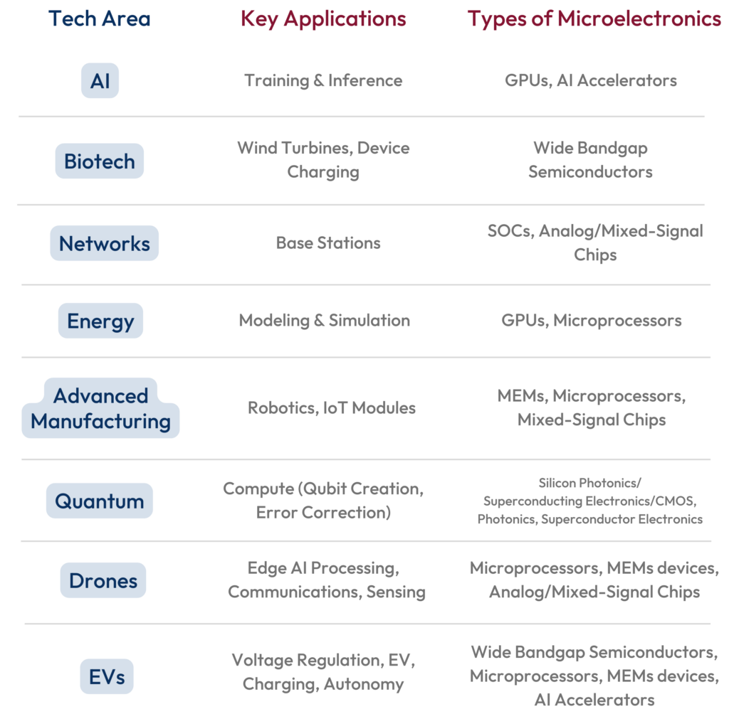
- Microelectronics Are a Key Enabling Technology for All Battleground Sectors. U.S. and allied competitiveness in AI, advanced networks, biotechnology, energy generation and storage, and convergence technologies like advanced manufacturing, drones, and EVs hinge on sustaining microelectronics innovation and growing compute power.
Moonshots are audacious goals that can move the entire U.S. innovation ecosystem toward a position of competitive advantage. These proposed goals are beyond “hard,” but like the Apollo Program they are attainable through a whole-of-ecosystem effort.[63] As the microelectronics industry approaches the end of Moore’s Law, the United States needs an Apollo-like effort dedicated to scaling and seamless integration of emerging compute paradigms. Such an approach would fulfill the vision of the 2017 Report to the President on Ensuring Long-Term U.S. Leadership in Semiconductors, which called for a ‘leapfrog’ strategy in compute and microelectronics to retain American competitiveness.[64] The CHIPS R&D program funded by the CHIPS & Science Act offers the nation an unprecedented opportunity to launch such programs.
What sets moonshots apart from more incremental approaches to technological progress? First, by aiming to achieve a step-change or paradigm shift, such programs drive the rest of the innovation ecosystem toward a vision of national advantage. Second, properly-designed moonshots promote accountability by assigning a National Mission Manager to own the program full-time. And third, moonshots aim to create a tangible platform – a capability – that solves an especially hard problem and creates many second-order benefits for the economy. The correct number and type of moonshots are ultimately determined through technology and competitive strategy arguments.[65]

1.1 Integrate Multiple Forms of Compute Via Hybrid Computing
The nation that creates integration among emerging compute paradigms will have a dominant advantage exiting this decade. As new forms of compute emerge as viable paths forward, the nation that scales multiple forms of compute and develops a method to make them seamlessly interoperable – both with CMOS and with each other – will be best positioned for a post-Moore’s Law world.[66] The overarching aim, therefore, should be a hybrid computing strategy that combines these modalities through a general-purpose CMOS ‘user interface.’ The result would be the ability to combine the strengths of each compute architecture in an interoperable way for applications like AI. Such an approach could enable supercomputing beyond exascale, sustainable AI in hyperscale data centers, and other demanding applications.
Objective: Create hybrid computing architectures that are seamlessly interoperable, addressing the complexity of extreme heterogeneous computing environments that are emerging to address challenging problems with incalculable societal impact. For example, such a system could integrate AI outputs across multiple compute paradigms, from conventional high-power CMOS to emerging compute paradigms based on novel hardware.
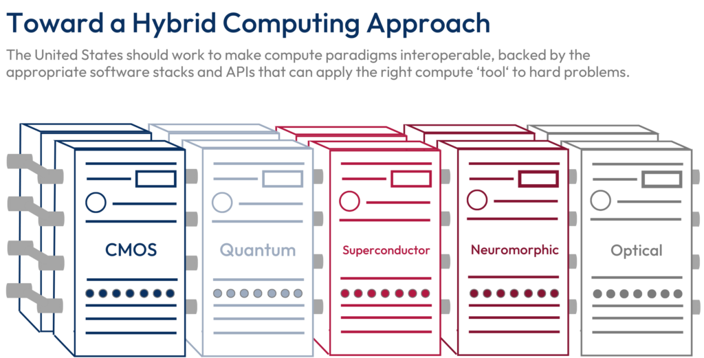
Method: Charge a National Mission Manager at the Department of Energy (DOE), NSTC, or an alternative responsible organization to create an integrated computer architecture that combines all three categories of computer for a national security application. Employ a co-design approach to create integrated hardware, firmware, and software to bring appropriate forms of compute to bear on various AI problem sets. In addition to creating a novel integrated hardware and software stack, develop a family of AI applications (or “system of systems”) with an application programming interface (API) gateway approach for specific computationally intensive national security applications. The chosen application could involve open-source intelligence fusion, modeling and simulation of national security scenarios, or military command and control recommendation agents. The resulting architecture would take the advantages of each form of compute and apply the AI sidecar best suited for the task.
1.2 Create a One Million Qubit Fault-Tolerant Quantum Computer by 2028
Quantum information science (QIS) has become like an economic sector unto itself.[67] Harnessing the power of the atom as a processor, quantum computing can offer a step-change in our ability to tackle compute-intensive tasks like advanced modeling.[68] For quantum computing, the remaining technical hurdles are not trivial, and include sensitivity to interference (error rates),[69] scaling challenges,[70] and unresolved interoperability challenges.[71] Commercial quantum computing R&D has spurred multiple startups and significant private investment in recent years, yet lengthy commercialization timelines, steep technical hurdles, a lack of proven use cases, and a volatile federal funding environment risk the onset of a “quantum winter” just as rival ecosystems double down on achieving large-scale systems.
Objective: Develop a one million qubit fault-tolerant computer with interconnect output to CMOS (potentially via a cloud accessible quantum hub) by 2028.
Method: The U.S. government should support a renewed National Quantum Initiative, including elevating it to the Office of the Vice President and naming a National Mission Manager as a direct report to the Vice President who will develop a strategy for the breakout and commercialization of quantum computing this decade, and providing necessary funding to the initiative. The initiative could update the 2018 national quantum strategy and should focus on identifying opportunities to scale public-private partnerships that provide startups access to enabling technologies like cryogenic refrigeration, as well as developing action plans for delivering on the stated quantum objectives between the United States and its allies and partners.[72] An updated strategy should also address the need to produce scalable quantum microelectronics domestically and secure other elements of the supply chain for quantum computing components.
1.3 Improve Compute Energy Efficiency by 1,000x to 1,000,000x
Since the mid-2000s, scaling in compute energy efficiency has slowed significantly.[73] This poses a major challenge at a time when AI workloads are rapidly accelerating compute demand: if current trends continue, energy demand from compute could exceed global energy generation by 2040.[74] Novel materials, devices, and architectures are needed to dramatically reduce energy consumption, and novel compute paradigms could make the most significant difference in the long term. Reversible computing, for instance, could alleviate this problem by harvesting energy that would otherwise be lost as heat, allowing for computations to occur below thermal limits of conventional hardware, and perhaps eventually below the Landauer Limit – the ultimate limit to scaling energy efficiency.[75]
Objective: Reduce energy consumption by 1,000x within 10 years while targeting a 1,000,000x reduction by 2040.[76]
Method: Launch a national moonshot program led jointly by the DOE’s Advanced Manufacturing office (AMO) and Office of Science, which have already established major research programs for the future of microelectronics, with involvement from the NSTC and relevant national labs.[77] Such a program should pursue a range of compute paradigms and relevant materials, devices, and architectures.[78] In particular, the program should focus on scaling for reversible computing by tackling core problems across the stack like developing novel algorithms, cell libraries, electronic design automation (EDA) tools, and fabrication techniques.[79] [80]
1.4 Lead in Superconductor Electronics
Superconductor electronics leverage the unique quantum properties of superconducting loops and switching devices called Josephson junctions to create extremely fast, energy-efficient circuits with zero electrical resistance.[81] Superconductor electronics accelerate classical computing, and also enable promising new approaches to neuromorphic computing, quantum computing, and reversible computing.[82] All told, this hardware paradigm carries the potential to unlock new forms of AI far surpassing present capabilities.[83] Recent breakthroughs in device density, memory elements, and design tools for superconductor electronics suggest that the technology may be approaching commercial readiness.[84]
Objective: Position the United States to lead the scaling of superconductor electronics by 2030, with a long-term goal of using these circuits in large-scale hybrid computing systems.
Method: Identify a National Mission Manager at the NSTC, DOE, or an alternative responsible organization responsible for taking key actions to scale superconductor electronics. Key moves should include:
- Opening a commercial-scale, 300mm wafer production line for superconductor electronics on American soil by 2030;
- Funding a national program that aims to interface superconductor electronics with photonics and CMOS to build a large-scale supercomputer.[85] Such hardware is uniquely conducive to large-scale computational systems leveraging digital, neural, and quantum principles;
- Increasing R&D efforts in superconductor neuromorphic architectures. Such a program should draw from biological systems, with an end goal of developing a new approach to AI capable of continuous learning;[86] and
- Developing a strategy with National Science Foundation (NSF), DOE, and the National Institute of Standards and Technology (NIST) to train 1,000 engineers in superconductor electronics by 2030, with a goal of unleashing innovation.[87]
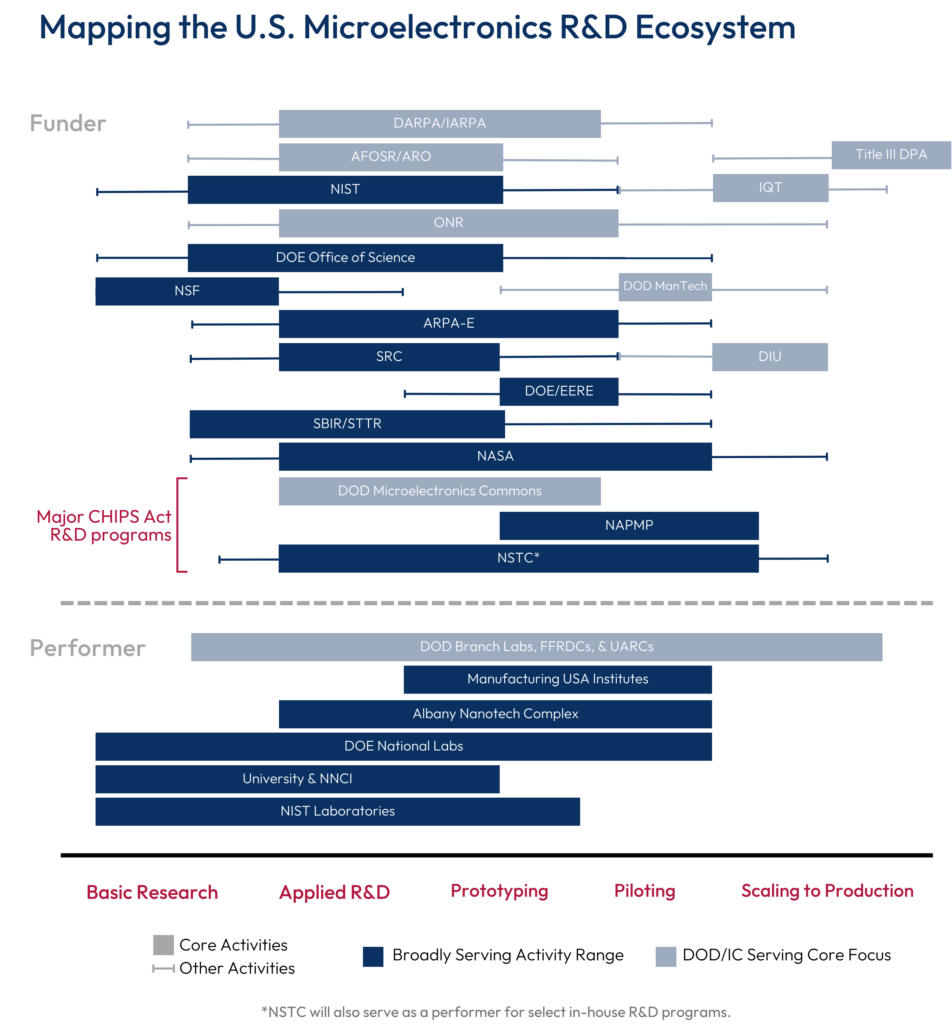
By all accounts, the United States enjoys the world’s most vibrant innovation ecosystem for compute and microelectronics. This ecosystem is anchored by research programs at several hundred colleges and universities,[88] many of which are funded by government players – including the NSF, DARPA, and the National Nanotechnology Initiative – and industry players such as the Semiconductor Research Corporation.[89] The Department of Defense (DoD), via DARPA, has historically played an outsized role in driving the future of microelectronics systems.[90] But the contemporary challenge has grown to transcend its DoD origins. At the same time, the innovation ecosystem has grown more decentralized as key hubs in the ecosystem – including MOSIS and SEMATECH – have retreated or dissolved, leaving university and government labs to pursue their research agendas with minimal national direction or scaffolding to translate innovation to commercial scale.[91] Meanwhile, industry players have pulled back long-term R&D efforts in favor of near-term process nodes as competitive pressures mount.[92]
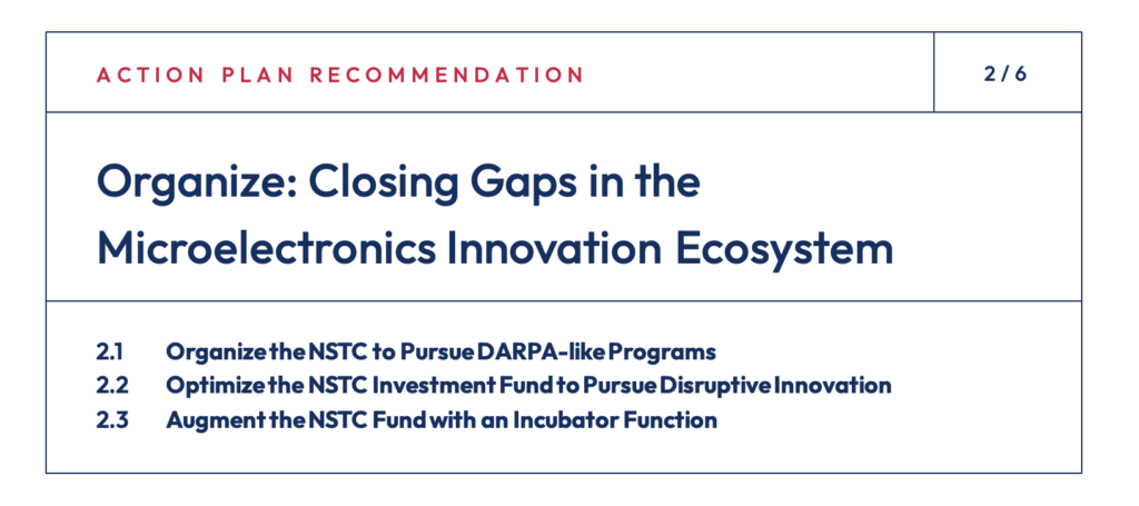
With the passage of the CHIPS & Science Act, the microelectronics R&D ecosystem has received a much-needed jolt. The National Microelectronics R&D Strategy is a positive step toward a coordinated, national approach to semiconductor R&D,[93] while new institutions like the NSTC, NAPMP, and DoD Microelectronics Commons will create additional capacity for prototyping – a major boon to researchers and innovators who often lack access.[94] Yet this organizational scaffolding is unlikely to be able to rise to the role of a NASA for microelectronics unless several significant gaps are filled: 1) a dedicated hub for compute and microelectronics moonshots; 2) a large investment fund, as authorized by the CHIPS Act; and 3) robust mechanisms to convene the private sector in pursuit of national priorities.
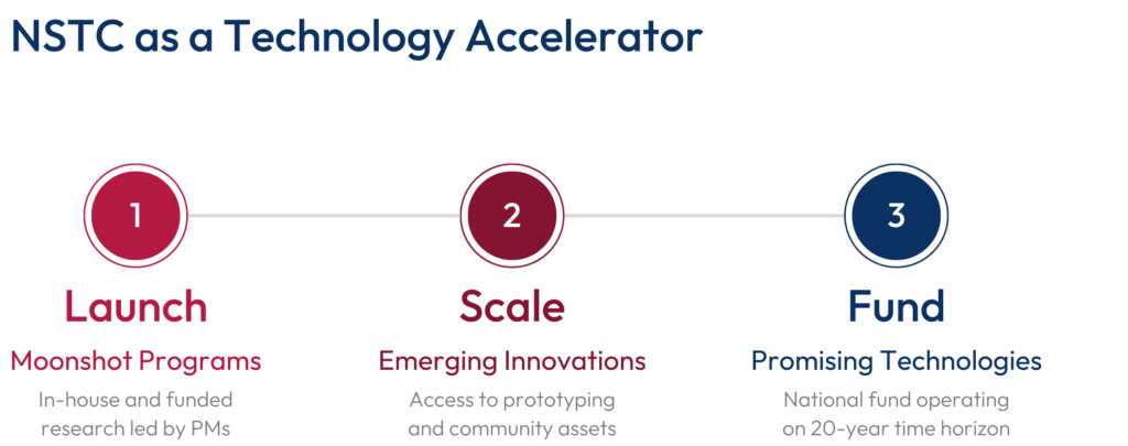
2.1 Organize the NSTC to Pursue DARPA-like Programs
The NSTC has been tasked by Congress and the Executive Branch with ensuring U.S. technological leadership in microelectronics over a 20-year time horizon.[95] Thus far, initial implementation focus has focused on offering access to prototyping capacity; providing community resources, such as access to design tools; and administering workforce development programs.[96] These initiatives address significant gaps in the innovation ecosystem. Access to prototyping in particular has been correctly identified as the core challenge to scaling microelectronics innovation in the United States.[97]
To guide this new organization, the Department of Commerce (DOC) has established an eminently qualified Industrial Advisory Committee (IAC) to guide CHIPS Act implementation.[98] Yet, in order to act as the nation’s premier research entity, the NSTC must also have the capacity and mandate to plan and execute future-oriented, national-level moonshot programs, in partnership with the private sector and other government entities. Spurring step-changes in compute and microelectronics, enabled by deep co-design, will require a DARPA-like approach backed by sufficient organization and resourcing.
Objective: Ensure the NSTC is positioned and organized to ensure U.S. technological leadership in compute and microelectronics over a 20-year time horizon by executing national, bar-setting programs.
Method: Structural characteristics that would allow NSTC to achieve these objectives include the following:
- Strong Central Hub. If the NSTC is to successfully pursue its research agenda and convene key players across the microelectronics ecosystem, it must be anchored by a strong central hub and connected to Centers of Excellence and prototyping facilities on the periphery.[99] The organizational hub could be split between several separate facilities to cover the full gamut of technologies emerging across the stack.
- Independent Technical Staff Augmented by Detailed Staff. Combining characteristics of imec and DARPA, the NSTC should have an in-house, independent technical staff to support Program Managers. Bringing in short-term industry and university detailees can support workforce training and facilitate tech transfer.
- Shielding From External Pressures. Historically, DARPA has been allowed to pursue its research agenda free from external pressures – an underrated key to its success.[100] NSTC must be afforded similar freedom to set its research agenda.
- Ability to Partner with Other Government R&D Programs. NSTC should not be limited to performing its own research. Instead, the organization can serve as a force multiplier that scales promising research programs through funding and convening.
2.2 Optimize the NSTC Investment Fund to Pursue Disruptive Innovation
The CHIPS & Science Act authorized the NSTC to launch an investment fund that, if implemented effectively, can provide patient capital to scale transformative innovations from across the compute stack. Entrepreneurs working on disruptive technologies in the microelectronics space face daunting challenges, including very high initial costs compared to other industries and an understandable reluctance among many venture capital (VC) firms to invest in hardware technologies with a consolidated market and an uncertain timeline to commercialization.[101] Since bets by even the most accomplished VC funds fail far more often than they succeed, an NSTC fund demands a higher-than-typical tolerance for uncertainty and risk.[102]
Objective: Launch a sufficiently resourced NSTC fund, potentially via an external partner, focused on de-risking seed and early-stage startups aiming to bring disruptive technologies from across the compute stack to market.
Method: Adopt best practices from notable deep tech investment funds, such as In-Q-Tel (IQT) and The Engine, as well as impact investing principles.[103] The fund should be shaped according to the following characteristics:
- Focus on Seed- and Early-Stage Investments. The most significant funding gap for disruptive technologies across the microelectronics stack exists earlier in the startup lifecycle. Investing early would unlock additional investment and encourage established funds to invest.[104]
- Robust Due Diligence and Professional Fund Management. Ensure professional and experienced private sector-based fund management and due diligence capabilities to optimize the quality and effectiveness of capital deployments, including through private sector matching. To ensure objectives are being met, incorporate necessary but streamlined monitoring, measuring, and reporting requirements. Direct partnerships with relevant investment organizations should not be ruled out.
- Adopt an “Evergreen” Structure. The fund should be structured such that returns from successful exits are reinvested in additional funding rounds or used to finance other critical NSTC programs, such as incubator support or long-term R&D programs.[105]
- Operate Over a 20-Year Time Horizon. Given long timelines to commercialization for innovation in the microelectronics stack (typically 10 to 20 years), the fund should operate over a 20-year time horizon, as opposed to the 10-year time horizon preferred by conventional venture funds.[106]
- $500 Million Initial Capitalization.[107] A larger fund will allow for additional shots on goal and offer additional flexibility to support scaling via larger Stage B funding rounds.
- Capital Allocation Council. Enabling private sector participation in the fund to provide seasoned technical expertise, evaluative discipline, and the strongest possible diligence. Select VC investors, horizon scanners, and technologists could be convened in an off-the-record, advisory fashion to support NSTC fund managers.
2.3 Augment the NSTC Fund with an Incubator Function
Navigating the microelectronics R&D and funding landscape can be a disorienting experience for innovators. Dozens of federal R&D programs – run seemingly in parallel and with limited connectivity – carry different requirements, grant applications, and government customers, creating hurdles that primarily impact small- and medium-size businesses. Once innovators develop a product, taking their technology to market can be an even more challenging experience. Institutionalized support is needed to increase the odds of successful commercialization.
Objective: Provide a dedicated “help desk” and commercialization support function for microelectronics researchers and innovators to lower barriers to entry.
Method: Establish an “incubator” program linked to the NSTC Investment Fund to offer commercialization support, access to cutting-edge equipment, and mentorship programs for microelectronics innovators. Dedicated commercialization support would increase the odds of success for the NSTC program and startups funded by the investment fund. Such a program should be modeled on approaches taken in recent years by established deep tech investment funds and agile government funders like IQT, DARPA, and the Defense Innovation Unit.[108]
Microelectronics ranks as one of the world’s most R&D-intensive industries: each year, about 19 percent of companies’ profits are immediately re-invested into R&D.[109] For decades, however, public investment in the field has remained relatively flat while industry R&D spending has ballooned.[110] This growing imbalance has shifted the nation’s research priorities from long-term breakthroughs towards short-term incremental improvements. Short-term industry R&D is important to develop and commercialize new process nodes, but the history of the chip industry shows that long-term pathfinding R&D is necessary to develop new technological paradigms.[111]Public R&D spending on microelectronics remains small compared to the roughly $50 billion that the chip industry spends every year on R&D, though the CHIPS & Science Act will go a long way towards addressing the imbalance.[112]
Public R&D spending tends to be a worthwhile investment because it brings additional private dollars with it. This virtuous cycle drives innovation, boosting productivity and GDP growth.[113] According to one estimate, every dollar in additional federal R&D spending raises total R&D spending by $8 by unlocking private investment.[114] But even this cycle is threatened: the U.S. tax code is unfavorable to capital- and R&D-intensive industries like microelectronics, driving chip companies to invest their R&D dollars elsewhere. Additional public funding could not only ensure long-term U.S. leadership in microelectronics, but would also pay significant economic and strategic dividends.
Graphic Source.[115]
3.1 Fuel Compute and Microelectronics R&D for Long-Term Competition
The decline of Moore’s Law has forced the semiconductor industry to spend more and more R&D funding on readying the next several technology nodes for production, rather than funding long-term research into novel and emerging paradigms.[116] Public R&D funding faces two key challenges: first, the Science portion of the CHIPS & Science Act authorizes significant funding increases for early-stage compute and microelectronics research, but this funding has yet to be fully appropriated. Additional public R&D funding for early-stage research is necessary to keep making breakthroughs in materials, devices, and architectures. And second, CHIPS R&D funding – which is focused primarily on applied research, prototyping, and scaling – is set to expire in 2027, leaving programs like the NSTC facing uncertainty and incentivizing a shorter-term focus. Greater assurance of sustained funding would encourage these programs to tackle moonshot goals.
Objective: Building on the groundwork laid by the CHIPS & Science Act, commit to ensuring durable U.S. leadership in compute and microelectronics by a) redoubling public support for basic research in relevant fields as the sector enters a new paradigm and b) providing sustained funding for CHIPS R&D efforts beyond 2027.
Method: Take steps to orient public R&D funding for long-term competition by:
- Fully Funding Significant Increases in Basic Research. Begin by fully funding microelectronics and compute R&D programs at the DOE, DoD, NIST, and NSF to the levels authorized by the Science portion of the CHIPS & Science Act.[117] In addition, Congress should fund the DOE’s Microelectronics Science Research Centers, as authorized by the CHIPS & Science Act.[118]
- Ensuring Sustained Funding for CHIPS R&D Programs. Works towards providing assurance that significant government funding for CHIPS R&D programs, such as the NIST’s Metrology R&D program, will continue beyond 2027. Metrology will play a crucial role in tackling the biggest technical challenges key to unlocking the next era of microelectronics innovation, including thermal management, materials characterization, hardware security, 3D stacking, and heterogeneous integration of exotic devices and materials. Sustained government seed funding will also be necessary to ensure the NSTC successfully achieves its objectives and to de-risk industry investment in the venture.
Developing Comparative Estimates for Microelectronics R&D Spending
Policymakers need reliable estimates for R&D spending in microelectronics and other battleground technologies – both in the United States and the PRC – to guide their investments in a budget-constrained environment. However, updated government estimates for federal microelectronics R&D do not currently exist.[119] This phenomenon also exists for other critical and emerging technologies, including AI, and is largely due to federal budget categories that are delineated by scientific fields, rather than technology categories.
To address this issue in the short term, Congress should commission a study to develop a concrete estimate of federal R&D spending on microelectronics and advanced compute.[120] To ensure the U.S. government is sufficiently organized in the intermediate term, SCSP has recommended the creation of an Office of Global Competition Analysis to conduct research and analysis for policymakers on matters pertaining to techno-economic competition, including comparative R&D spending.[121]
3.2 Crowd-In Industry R&D Funding Through Tax Policy
Federal R&D will not be enough to ensure U.S. leadership in advanced compute and microelectronics: the United States must also become the most attractive place for large chip companies to invest their R&D dollars. The best way to do this is through the tax code. Current U.S. tax code is unfavorable to the semiconductor industry, incentivizing companies to focus on current product lines and spend their R&D dollars outside the United States.[122] Unlike most chip-producing nations, America’s R&D tax credit does not allow firms to immediately expense R&D spending and, because it does not apply to R&D capital equipment, provides little value to the semiconductor industry. Plus, as of 2020, the United States ranked just 24th out of 34 OECD nations in terms of R&D tax credit generosity.[123]
Objective: Make the United States the most attractive nation for large semiconductor companies to invest their R&D dollars by providing competitive R&D incentives.[124]
Method: Rapid action by Congress could incentivize large semiconductor firms to invest their R&D dollars in the United States. Congressional action should be taken to double the Alternative Simplified Credit, an R&D tax credit, from 14 percent to 28 percent for strategic technology sectors.[125] Urgent action is also needed to restore full expensing for equipment purchases, a five year provision under the 2017 Tax Cuts and Jobs Act that has since lapsed.[126] Given that tooling in the semiconductor industry can cost between tens and hundreds of millions of dollars per machine, these moves would significantly increase U.S. competitiveness.[127]
Microelectronics design and fabrication requires a range of sophisticated tools, equipment, and processes. EDA tools, for example, are required to design working electronic circuits on chips that contain billions of transistors. During the fabrication process, each chip goes through over 1,000 steps, many of which require specialized equipment.[128] These enabling technologies are vital to continued compute scaling. In emerging paradigms, enabling technologies are often immature and must be developed in tandem with enabling technologies themselves.
4.1 Unleash AI-Powered Chip Design Tools
GenAI and the more general forms of AI that may emerge have enormous potential to help redesign key aspects of the microelectronics stack. The technology offers a pathway to cut the time it takes to design a chip from months to weeks or even days, while unlocking natural language rather than specialized programming languages as an input.[129] Some of this is not new.[130] However, we are now seeing how GenAI will combine with other specific AI fronts and advanced compute in this decade (e.g., quantum, neuromorphic, and biological computing). If applied to emerging hardware paradigms, like superconductor electronics, these powerful forms of AI tools could unlock significant new breakthroughs.
Objective: Expand and apply the combination of U.S. leadership in chip design tools and GenAI to heterogeneous integration and emerging paradigms, such as photonics, superconductor electronics, and quantum computing.
Method: Each national moonshot program and R&D effort in emerging compute paradigms should pair compute, chip, and manufacturing designers with AI specialists to accelerate prototyping and manufacturing of new capabilities. Additional de-risking through federal R&D programs, in partnership with industry, is also needed to operationalize this technology.
4.2 Build Digital Twins for Compute & Microelectronics R&D
Investment in physics-based simulated environments could help enable a true atoms-to-architectures innovation pipeline while accelerating compute and microelectronics R&D. Advanced physics-based digital twins would enable deep co-design processes that span from materials to large-scale compute systems, allowing for modeling and optimization before designs are prototyped in the physical world.[131] To make this a reality, additional research is needed for multiphysics modeling; simulation of complex large-scale environments, such as a high-yield semiconductor production line; and tightening the feedback loop between theory and experimentation in this area.[132]
Objective: Create digital twins of state-of-the-art microelectronics R&D facilities to enable atoms-to-architectures co-design and dramatically expand access to fabrication tools and prototyping capacity.
Method: NSTC hub data and facilities should be leveraged to create a digital twin/cloud lab for microelectronics research and prototyping, greatly expanding the reach of the program.[133] This effort should be launched under a public-private partnership model, overseen and administered by a third-party industry group yet buttressed by data generated via NSTC research. Access should be available to government, industry, and academic players that meet specified conditions, such as security screening, with upfront costs kept low to enable academia and startups to participate.
4.3 Scale the Materials Genome Initiative for AI-Enabled Materials Discovery
The past 15 years have witnessed a quiet revolution in materials science, with groundbreaking progress made in fields such as magnetic materials, 2D materials, carbon nanotubes, and topological materials.[134] Novel manufacturing processes allow these materials to be grown with atomic precision. Yet these breakthroughs often face a 10 to 20 year commercialization timeline, especially in the microelectronics industry. To address this disconnect, the Materials Genome Initiative (MGI) was launched by the White House in 2011 to “accelerate the discovery, design, development, and deployment of new materials, at a fraction of the cost, by harnessing the power of data and computational tools in concert with experiment.”[135] Yet competition in this space has intensified: the PRC has launched a parallel Materials Genome Engineering project backed by dedicated, large-scale scientific infrastructure for AI-enabled materials discovery and characterization.[136]
The advent of a more general form of AI, coupled with advances in quantum computing that will unlock precision modeling at the molecular level, has made MGI’s ambitious goal of revolutionizing materials science through tightly integrated modeling and experimentation much more achievable by 2030. Deep learning allows for training on massive amounts of data – even a relatively small model can ingest the entire arXiv repository in less than 24 hours.[137] GenAI allows for the autonomous generation of materials candidates, which can then be evaluated by human experts and tested in self-driving “cloud labs.”[138]
Objective: Scale the MGI, capitalizing on America’s lead in GenAI to transform materials science. Integrate MGI more closely with the U.S. microelectronics innovation ecosystem and provide a clear pathway for materials to reach commercialization.
Method: Provide a significant funding increase for MGI to enable the program to capitalize on recent developments in GenAI. In addition, the DOC should create a national center of excellence at the intersection of advanced materials and microelectronics. Such a center could coordinate MGI efforts relevant to semiconductors and would be responsible for convening the private sector, academia, and relevant government players. A national center could be established either as one of the NSTC’s planned technical centers or as a ManufacturingUSA Institute funded under the CHIPS Act.[139]
4.4 Reshape Microelectronics Fabrication via Fab-in-a-Box Approaches
Advances in machine learning, precision additive manufacturing, colloidal chemistry, and bottom-up fabrication for nanoelectronics have opened the door to significant disruptions to the chip manufacturing process. Entire transistors, for example, may conceivably be mass-produced through a growth process – similar to how chemicals are manufactured today – and suspended in an ink. Then, circuits could be created by an additive manufacturing "pen" guided by a specially trained AI model.[140] This ambitious endeavor (and other similar approaches) could unlock microelectronics fabrication in distributed mini-fabs.[141] Significantly reducing the cost of building a fab would also lower barriers to entry for new players, helping to reverse a decades-long trend towards industry consolidation.
Objective: Develop fundamentally new approaches to fabricating microelectronics. Catalyze a 1,000x or greater improvement in cost and/or footprint, as well as flexible manufacturing processes to create custom circuits on-demand.[142]
Method: Launch a national program, based at the NSTC or an alternative R&D agency, tasked with developing and vetting process technologies that challenge fundamental assumptions in today’s microelectronics fabrication process. For example, portable mini-fabs could theoretically print custom circuits on-demand at trailing-edge nodes in minutes rather than the weeks it requires today. While these methods may not produce bleeding-edge chips for AI applications, they promise other exciting opportunities, including new circuit topologies and form factors, natural heterogeneous integration at the microscale, circuits extensible in space and time, and streamlined translation of R&D advances into manufacturing.[143] Alternatively, such a capability could serve as a flexible and adaptable research platform for related microelectronics technologies such as micro-electromechanical systems (MEMS), photonics, and sensors.
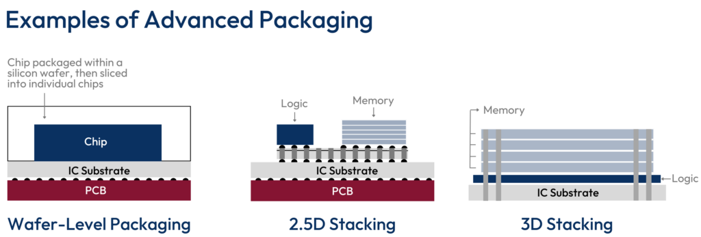
4.5 Pursue Technological Leadership in Advanced Packaging & Chiplets
Advanced packaging – the ability to stack chip components on top of one another and connect them in novel ways – enables 3D heterogeneous integration and, as such, is becoming a key factor in microelectronics technology leadership.[144] However, more than 60 percent of packaging and test capacity is located in Taiwan and China, while the United States “lacks any large-scale, commercial state-of-the-art advanced packaging capability.”[145] Today, just three percent of advanced packaging capacity is located in North America.[146]
Advanced packaging enables the combination and stacking of small, modular chips known as chiplets. Each chiplet represents a particular function, which can be combined together to form a complete microelectronic system. While chiplets have been implemented in large vertically integrated companies, creating an open marketplace for chiplets that allows buyers to “mix-and-match” components for specific use cases would unlock innovation and create more opportunities for small companies.[147]
Graphic Source.[148]
Objective: By 2030, position the United States as the driver of global innovation in advanced packaging technologies, including by facilitating creation of an open chiplet ecosystem and sustaining leadership in silicon photonics. Prioritizing innovation in tandem with a planned packaging capacity buildout is more likely to achieve both technological leadership and increasing production capacity than if either of these objectives are pursued alone.[149]
Method: In addition to making significant investments in domestic packaging capacity as part of the CHIPS & Science Act,[150] DOC and other R&D funding agencies should prioritize packaging R&D in areas such as glass substrates, high-density interconnects, and process automation. Applied research and prototyping in silicon photonics should be prioritized as part of the NAPMP and NSTC programs. Additional future support – including tax credits and loans – for domestic packaging, as well as IC substrate capacity, should not be ruled out.[151]
Moves to facilitate the creation of an open chiplet ecosystem include the following:
- NIST should define technical standards for chiplets, in partnership with international industry partners, in a way that enables U.S. firms and entrepreneurs to lead; and
- NSTC should create a testing platform, based on a common set of standards and featuring a shared interface, to evaluate performance claims for chiplets.
4.6 Unleash Next-Generation Lithography by Deepening Public-Private Partnerships
Next-generation lithography techniques and advanced light sources are a technology wildcard which could grant chip companies based in the United States a significant manufacturing edge.[152] But this competition is not taking place in a vacuum: the PRC recently announced that it would build multiple industrial-scale chip factories around particle accelerators in an attempt to circumvent U.S. and allied restrictions on advanced chip tooling.[153]
Objective: Harness the U.S. advantage of national particle accelerators at DOE labs to commercialize next-generation advanced lithography techniques.
Method: The technology and infrastructure developed in U.S. national laboratories for particle accelerators can be used by private sector companies to augment existing lithography tools, turning advanced light sources into an industrial “utility.” The DOE should establish Cooperative Research and Development Agreements (CRADAs) with U.S. companies that can develop prototype tools by way of an open competition, with an end-goal of outfitting multiple research- and industrial-grade facilities.[154] In addition, relevant funding agencies should explore the creation of a “national resource” for advanced light-based (lithography, metrology, and inspection) techniques to foster process innovation in microelectronics.
4.7 Offer Cryogenic Refrigeration as a Service
Today’s quantum computers and most superconductor electronics must be cooled to extremely cold temperatures, just a few degrees from absolute zero. To reach these temperatures, firms must purchase specialized cryogenic refrigeration units that can cost upwards of several million dollars.[155] These high initial costs present a significant barrier to entry for new players seeking to enter the quantum computing and superconductor electronics space.
Objective: Make refrigeration as a service widely available to companies, especially startups, based in the United States and allied nations.
Method: Via the National Quantum Initiative, coordinate the signing of Cooperative Agreements between industry players and relevant U.S. government agencies,[156] including the DOE and NIST.[157] Startups based in the United States and National Technology Industrial Base (NTIB) countries should be eligible to participate.
Microelectronics is a global industry supported by the world’s most complex supply chain: on average, each segment of the semiconductor value chain includes players from 25 nations.[158] Ever since chip shortages rocked the global economy in 2021, semiconductors have found their way onto the agenda for international dialogues. White House-led efforts have resulted in several major deliverables, including bilateral partnerships with Vietnam, India, and Japan, as well as collaboration on the semiconductor supply chain through IPEF and the TTC[159] Building on these efforts, the next opportunity for allied coordination is addressing shared cybersecurity risks stemming from the proliferation of cheap, insecure legacy chips, IoT devices, and other hardware security vulnerabilities.
The intersection of emerging hardware security challenges with China’s rise as the world’s leading producer of chips at legacy nodes has created a new and challenging cybersecurity risk vector.[160] Over the next several years, PRC firms intend to build out nearly as much capacity at these nodes as the rest of the world combined.[161] As noted above, malign actors can plausibly insert vulnerabilities, such as hardware trojans, into systems at the design or fabrication stages. These vulnerabilities are extremely difficult to detect.[162] If an adversary produced lagging-edge chips or chiplets that are compromised, then sold them to critical infrastructure providers, it could enable targeted or large-scale cyberattacks intended either to exfiltrate data or disable or degrade performance of connected devices.[163]
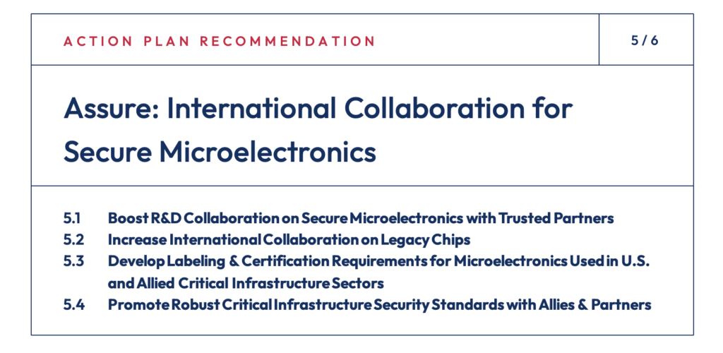
5.1 Boost R&D Collaboration on Secure Microelectronics with Trusted Partners
As cybersecurity risks to the hardware layer proliferate, microelectronics must be designed with security in mind. Innovation in these areas can be supercharged through public-private partnerships and international R&D collaboration with trusted partners.[164] For example, Arm’s Morello project is a public-private partnership between Arm, Stanford University, and Cambridge University, focused on developing a more secure CPU architecture, that has received funding from DARPA and the United Kingdom’s (UK’s)’s Industrial Strategy Challenge Fund.[165] Innovation in hardware security technologies is also a crucial enabler for compute governance mechanisms for AI.[166]
Objective: Create a force multiplier for secure microelectronics R&D by increasing international collaboration.
Method: U.S. R&D funding agencies, including NIST and NSF, should jointly fund R&D collaboration on secure-by-design microelectronics with allied nations such as the UK, Japan, Australia, Taiwan, and South Korea. These areas would also be ideal investments for the Department of State’s International Technology Security and Innovation Fund established under the CHIPS Act.[167] Initial areas for investment could include:[168]
- Trusted execution environments
- AI-enabled verification and validation, including hardware trojan detection
- Physically unclonable functions & secure roots of trust (e.g., for supply chain traceability)
- Tamper-proof packaging
- Secure chiplets
- Side-channel-resistant architectures
- Processes for implementing and enforcing secure-by-design principles
- Privacy-protecting technologies, such as fully homomorphic encryption
The Executive Branch could also create a public-private partnership designed to deepen collaboration in this space via fellowship programs. For example, the DoD and the State Department could partner with R&D funders such as the Semiconductor Research Corporation to launch an international R&D fellowship program focused on secure microelectronics open to scientists from NTIB countries.[169] A DoD-led program could place technical fellows at government research programs (such as DoD’s Microelectronics Commons), university research centers,[170] and major industry players.
5.2 Increase International Collaboration on Legacy Chips
The PRC is subsidizing massive capacity buildouts for legacy chips,[171] which are utilized for a variety of general purpose microcontrollers, including IoT devices and 95 percent of automotive chips.[172] Major democratic market economies including the European Union (EU), Japan, South Korea, and the United States should join forces to insulate their markets, guard against security risks, and avoid deepening reliance on heavily subsidized PRC lagging-edge chips.
Objective: Create a level playing field for chipmakers in the United States and allied and partner countries by adopting a ‘market demand pooling’ strategy for lagging-edge microelectronics.[173]
Method: Elevate policy coordination on legacy chip production in fora such as bilateral dialogues with Germany, Japan, South Korea, Taiwan, and the TTC; trilateral trade meetings between the United States, the EU, and Japan; and other dialogues with allies and partners.[174] As a first step, a group such as the United States, the EU, Japan, and South Korea should jointly should assess the economic andand national security implications of China’s massive capacity buildout for trailing- and lagging-edge chips, including hardware security issues stemming from their likely deployment throughout critical infrastructure sectors in democratic market economies.[175] The United States and its allies and partners should also consider policy measures such as common or coordinated security protocols – developed with input from appropriate industry bodies – and coordinated use of trade tools, including tariffs.
Graphic Source.[176]
5.3 Develop Labeling and Certification Requirements for Microelectronics Used in U.S. and Allied Critical Infrastructure Sectors
Many firms servicing critical infrastructure sectors possess limited visibility into their own supply chains and may be unaware of the origins of electronic components in their systems.[177] Restrictions on DoD purchases of chips produced by countries of concern were included as part of the 2023 National Defense Authorization Act (NDAA), but these restrictions contain considerable loopholes, do not apply to critical infrastructure sectors, and do not go into effect until 2027.[178] Additional mechanisms are needed to assess and manage risk to these sectors from microelectronics produced in the PRC.
Objective: Assess and mitigate risk to critical infrastructure – in both the United States and among allies and partners – stemming from microelectronics and other electronic components produced in countries of concern.
Method: Steps that could be taken through either Congressional and/or Executive action include:
- Increase Transparency by Requiring a Hardware Bill of Materials (HBOM):[179] Require firms servicing U.S. government customers and critical infrastructure providers to disclose country-of-origin and other information on hardware components via an HBOM. This measure would be a critical first step toward providing much-needed supply chain transparency[180] and would allow for cybersecurity vulnerabilities at the hardware or firmware level to be resolved more rapidly.[181] Building on its recently released HBOM Framework for Supply Chain Risk Management,[182] the Cybersecurity and Infrastructure Security Agency (CISA), in collaboration with NIST, should be directed to develop guidelines for HBOM disclosures. The State Department and NIST should engage with U.S. allies and partners on this requirement as part of a diplomatic initiative on cybersecurity at the hardware level.
- Assess Risk to Critical Infrastructure by Flagging High-Risk Chips: The DOC, with support from relevant sector risk management agencies, should create a three-tier certification system to classify microelectronics destined for critical infrastructure sectors as high-risk, medium-risk, and low-risk. DoD’s work on secure supply chain methodologies – such as the Trusted Foundry and Microelectronics Quantitative Assurance models – should be leveraged where feasible to ensure design security and testing and validation checks.[183] The 2019 Executive Order on Securing the Information and Communications Technology and Services Supply Chain could also be used to restrict purchases from high-risk suppliers.[184]
5.4 Promote Robust Critical Infrastructure Security Standards with Allies and Partners
Setting security standards is an essential move to promote hardware security for critical infrastructure, and this effort must be done with allies and partners to be effective. Attention should be paid to the entire hardware stack, from IoT modules to the chips which power these devices. Passed in 2020, the IoT Cybersecurity Act was the first piece of U.S. legislation to address the cybersecurity of IoT devices, but more work remains to be done to address critical infrastructure or secure microelectronics at home and abroad.[185]
Objective: Expand security standards for IoT cybersecurity to critical infrastructure sectors, including a focus on hardware and firmware.
Method: Take both domestic and diplomatic action, including:
- Domestic: Fully implement the IoT Cybersecurity Act of 2020 by releasing cybersecurity standards for critical infrastructure sectors. NIST has addressed cybersecurity guidance aspects of the IoT Cybersecurity Act,[186] but is also required to develop sector-specific standards in coordination with the CISA, sector risk management agencies,[187] and industry.[188] Future efforts to develop these standards should include a robust line of effort on hardware security.
- International: Developing IoT standards for critical infrastructure would be much more effective if done in consultation with allies and partners. The State Department, in consultation with NIST, should engage with allies and partners to strengthen security standards for critical infrastructure. In addition, hardware cybersecurity should be prioritized as a line of effort at international dialogues with allies and partners such as Taiwan, the EU, South Korea, and Japan.
Talent is a key enabler that underpins the nation’s competitiveness in any international technology battleground. Even as human-machine teaming transforms the way science is done, human intuition, communication, and abstract reasoning will always be at the center of how America innovates. The United States must set the path today to develop, attract, and retain a world-class workforce across the various disciplines that drive microelectronics innovation.
Currently, the United States faces a significant shortage of technicians and engineers needed to staff fabs – some estimates place this shortage at approximately 90,000 workers.[189] Several academic-industry consortia,[190] led by universities like Purdue, Arizona State University, and the Ohio State University, have launched programs to provide training from the Associates’ to PhD levels.[191] To scale emerging paradigms and promote disruptive innovation, however, the nation must focus beyond staffing fab positions to training future research talent.
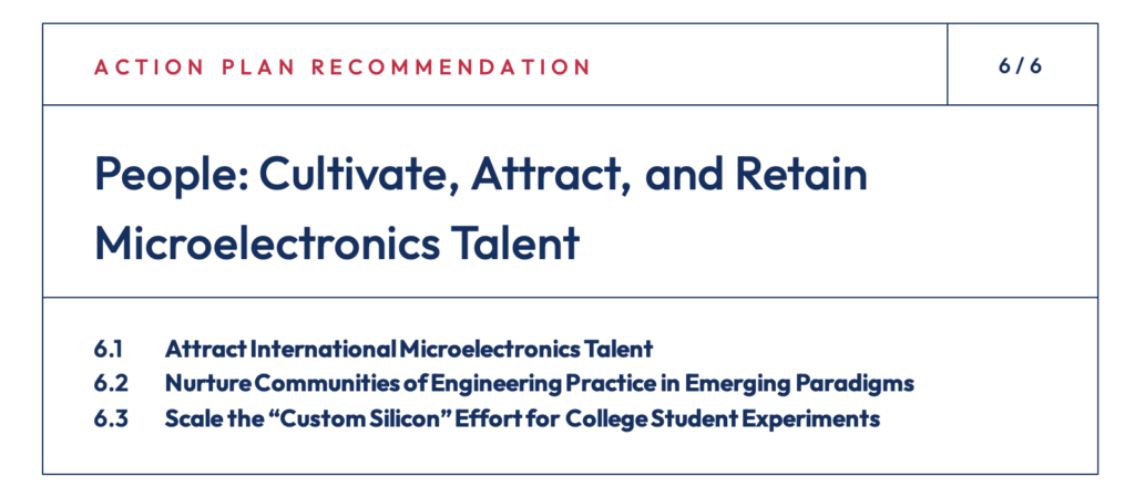
6.1 Attract International Microelectronics Talent
Roughly 40 percent of America’s high-skill microelectronics workers were born abroad.[192] Yet outdated high-skill immigration policies force many of these microelectronics workers to return to their home countries. With impending workforce shortages in both research and fab operation, creating clear pathways for microelectronics talent to study and work in the United States must be treated as a national imperative.
Objective: Create clear pathways to attract and retain the world’s top microelectronics talent by improving high-skill immigration.
Method: Congress should take steps to bolster the pipelines for international microelectronics talent, including:
- Exempt PhD holders in relevant fields from the current H-1B visa cap;
- Grant green cards to STEM PhD students graduating from accredited U.S. universities who intend to work in the microelectronics industry;
- Develop an “innovator” visa category, similar to the UK’s and Australia’s Global Talent Visa programs, for high-skilled immigrants working in the chip industry.[193]
6.2 Nurture Communities of Engineering Practice in Emerging Paradigms
Emerging compute paradigms are characterized by tight-knit research communities with specialized knowledge and skills. To this point, however, these communities have received minimal support from U.S. policymakers. Targeted intervention could grow the reach of these communities and expand their ranks.
Objective: Provide resources and support for communities of engineering practice in emerging paradigms.
Method: The DOC should take the following actions:
- Convene and support roadmapping efforts for emerging paradigms at NSTC facilities;
- Commission new textbooks and course materials for novel paradigms like superconductor electronics;[194]
- Develop an “atlas” of job descriptions and necessary skills for the chip industry, linked to training programs and courses that students should take;
- In coordination with the Department of State, launch a “Fulbright for NSTC” program to bring skilled researchers from trusted institutions to collaborate on national moonshot programs.
6.3 Scale the “Custom Silicon” Effort for College Student Experiments
During the early 1980s, CMOS emerged as the leading paradigm for silicon microelectronics thanks to new opportunities for students to learn and experiment with building their own chips.[195] DARPA’s MOSIS program, launched in 1981, enabled students to design chips and get them shipped for free.[196] This program, in turn, catalyzed breakthroughs in design tools that unleashed U.S. innovation. Providing similar opportunities today could catalyze a new generation of future semiconductor researchers and engineers and help spark new breakthroughs.
Objective: Create new opportunities for students to experiment with cutting-edge microelectronics by scaling the custom silicon movement.
Method: U.S. R&D funding agencies, including NSF, DOC, and DARPA, should scale public-private partnerships that provide students with as much hands-on experience designing and building their own chips as possible. For example, Google has teamed up with Global Foundries, Skywater, and startup Efabless on a Custom Silicon effort that allows anyone to design their own chips.[197] These tools should be supercharged with generative AI so that natural language can be used as an input.
Appendix A
Additional Elements of Success
Continued leadership in advanced compute and microelectronics is not assured. Success depends on many factors and efforts, some of which are already ongoing and lie out of the scope of this action plan. Additional elements of success include:
- The CHIPS & Science Act must restore some advanced semiconductor fabrication back to the United States. The National Security Commission on Artificial Intelligence called for maintaining multiple sources of cutting-edge microelectronics fabrication inside the United States to restore leading-edge chip fabrication on American soil.[198] This policy has remained largely constant, with Commerce Secretary Gina Raimondo calling earlier this year for at least two clusters of leading-edge logic in the United States.[199] By mid-decade, the world’s most advanced process nodes may once again be fabricated on American soil.
- The NSTC and DoD’s Microelectronics Commons program should combine to establish meaningful prototyping capacity in the United States. These programs can successfully unlock prototyping capacity for both specialty wafer runs and industry standard 300mm wafer runs, creating additional opportunities for startups and researchers.
- Government intervention and current U.S. leadership in chip design can propel U.S. firms to leadership in chip specialization. U.S. firms enjoy an overwhelming lead in chip design. As the chip industry increasingly shifts towards building specialized accelerators for key applications like AI, the combination of market incentives and federal R&D spending will help to keep U.S. firms at the forefront.
- Ensuring leadership in edge applications is critical. Chips for edge applications, like robotics, IoT modules, cars, and 5G base stations, require extremely low-power designs and mix digital and analog components in the same package. The PRC’s push for dominance in these sectors will extend to the underlying microelectronics. Leadership cannot be left to chance.
- Protect actions in compute and microelectronics are warranted, but running faster is also necessary for sustained U.S. advantage. The United States faces a determined competitor that brings substantial resources and sophisticated espionage and industrial capabilities to the table. As such, the PRC will likely make gains in key microelectronics verticals. Technology protections and common sense guardrails like research security policies are essential, and must be supported with sufficient resources and tools to enable robust implementation,[200] but these guardrails are no substitute for an acceleration of innovation by the United States and its allies and partners.
Endnotes
[1] See, e.g., Tristan Holtam, As Chipmakers Assess “Where” to Build New Fabs, the “How” of Semiconductor Innovation Must Remain a Priority, Applied Materials (2023).
[2] Timothy F. Bresnahan & Manuel Trajtenberg, General Purpose Technologies: "Engines of Growth?", National Bureau of Economic Research (1992).
[3] David Grossman, How Do NASA's Apollo Computers Stack Up to an iPhone?, Popular Mechanics (2017).
[4] John Shalf, The Future of Computing Beyond Moore’s Law, Philosophical Transactions of the Royal Society (2020); James R. Powell, The Quantum Limit to Moore's Law, Proceedings of the IEEE (2008).
[5] As historian Chris Miller notes, “most of the world’s GDP is produced with devices that rely on semiconductors.” Chris Miller, Chip War: The Fight for the World’s Most Critical Technology, Simon & Schuster at 23 (2022).
[6] Neil C. Thompson, et al., The Importance of (Exponentially More) Computing Power, arXiv (2022).
[7] Advanced compute can be defined as “computer systems where processing power, memory, data storage and network are assembled at scale to tackle computational tasks beyond the capabilities of everyday computers.” Independent Review of The Future of Compute: Final Report and Recommendations, UK Department for Science, Innovation & Technology (2023).
[8] Nerissa Draeger, Happy 150th Birthday to the Periodic Table, Lam Research (2019); Chapter 2: Energy Efficiency, MAPT: Microelectronics and Advanced Packaging Technologies Roadmap, Semiconductor Research Corporation at 47 (2023).
[9] See Decadal Plan for Semiconductors: Full Report, Semiconductor Research Corporation at 6 (2020); Catherine D. Schuman, et al., Opportunities for Neuromorphic Computing Algorithms and Applications, Nature Computational Science at 16 (2022). In a post-Moore's Law world, co-design is necessary to drive innovation across each layer of the stack simultaneously. See Cherry Murray, et al., Basic Research Needs for Microelectronics, U.S. Department of Energy at 8 (2018).
[10] Several large-scale studies and initiatives exist in this space. IEEE’s Rebooting Computing Initiative formed in 2013 in response to concerns that transistor scaling was nearing its limits. It manages the authoritative International Roadmap for Devices & Systems. IEEE Rebooting Computing Task Force, IEEE (last accessed 2023). A 2017 White House report authored by the President’s Council of Advisors on Science & Technology called for a “leapfrog” strategy to maintain U.S. competitiveness in compute and microelectronics, outlining several moonshots that the nation could pursue. Report to the President: Ensuring Long-Term U.S. Leadership in Semiconductors, President’s Council of Advisors on Science and Technology (2017). The Semiconductor Research Corporation released an authoritative Decadal Plan in 2020 outlining five “seismic shifts” that the semiconductor industry must navigate, alongside five “grand goals” that aim to accomplish this. Decadal Plan for Semiconductors: Full Report, Semiconductor Research Corporation (2020). DARPA’s Electronics Resurgence Initiative and Electronics Resurgence Initiative 2.0 have organized an ecosystem around 3D heterogeneous integration while tackling key challenges like hardware security. Electronics Resurgence Initiative 2.0, Defense Advanced Research Projects Agency (last accessed 2023). A 2022 PCAST report highlighted ways that the CHIPS Act could be used to strengthen the U.S. innovation ecosystem for microelectronics. Report to the President: Revitalizing the U.S. Semiconductor Ecosystem, President’s Council of Advisors on Science & Technology (2022).
[11] See Harnessing the New Geometry of Innovation, Special Competitive Studies Project at 30-32 (2022); Michael E. Porter, What Is Strategy?, Harvard Business Review (1996).
[12] Harnessing the New Geometry of Innovation, Special Competitive Studies Project at 30 (2022).
[13] Flagship industry roadmaps have identified a variety of emerging candidates for post-CMOS materials, devices, and architectures. Post-CMOS switch devices identified by the International Roadmap for Devices and Systems as areas for future research include NEMS Switches, Mott Devices, Topological Insulator-based Electronics, Negative Gate Capacitance FETs, Spin Wave Devices, Excitonic Devices, and various emerging magnetoelectric logic and memory devices. See Beyond CMOS & Emerging Materials Integration, International Roadmap for Devices & Systems: 2022 Edition at 1-36 (2022). The Heterogeneous Integration Roadmap highlights Nanoscale Vacuum Electronics, Neuromorphic Devices, Printed Electronics, Spintronic Devices, Graphene and 2D Material Electronics, Carbon Nanotube Electronics, and Plasmonic Devices as potentially high-impact. See Chapter 16: Emerging Research Devices, Heterogeneous Integration Roadmap: 2023 Edition, IEEE (2023).
[14] Vaclav Smil, July 1958: Kilby Conceives the Integrated Circuit, IEEE Spectrum (2018).
[15] Gordon Moore, Cramming More Components Onto Integrated Circuits, Proceedings of the IEEE (1965). Moore’s original prediction was that transistor counts would double every year, but he later revised this estimate up to doublings approximately every 18 to 24 months. Moore’s prediction also included regular cost decreases.
[16] A few of these breakthroughs included copper interconnects, a new 3D transistor design (FinFET), and extreme ultraviolet lithography (EUV). Hassan Khan, Scaling Moore’s Wall: Existing Institutions and the End of a Technology Paradigm, Carnegie Mellon University at 65-73 (2017).
[17] At present, industry roadmaps anticipate at least a decade of continued transistor scaling. As firms eye the 3nm node, a new 3D transistor called Gate-All-Around will use stacked nanosheets to deliver increased performance and power. Towards the end of the decade, firms plan to incorporate a 3D transistor design called CFET that stacks two layers of transistors directly on top of one another. Beyond these exotic transistor designs, the chip industry has targeted transistors made with low-D materials, including 1D carbon nanotubes and 2D materials called TMDs. These materials measure in at just a single atom thick. See Mark Lapedus, Transistors Reach Tipping Point at 3nm, Semiconductor Engineering (2022); Marko Radosavljevic & Jack Kavalieros, 3D-Stacked CMOS Takes Moore’s Law to New Heights, IEEE Spectrum (2022); Sajedeh Manzeli, et al., 2D Transition Metal Dichalcogenides, Nature Reviews Materials (2017); Max C. Lemme, et al., 2D Materials for Future Heterogeneous Electronics, Nature (2022). These exotic transistor designs could be paired with improvements in lithography. Extreme ultraviolet (EUV) lithography is scheduled to be upgraded with High-NA and Hyper-NA versions in the coming years. This technology could be boosted by improvements in the light source. Improvements in other alternatives, like nanoimprint lithography, could also help push the frontier. Canon Tries to Break ASML’s Grip on Chipmaking Tools, The Economist (2023).
[18] Dennard’s Law suggests that, as transistor scaling decreases the size of devices, energy consumption shrinks as well. Dennard scaling died around the mid-2000s, when processor clock speeds could no longer be increased without overheating the chip. In response, semiconductor firms rolled out multi-core processors that allowed them to keep pace with Moore’s Law in terms of performance. See Robert H. Dennard, et al., Design of Ion-Implanted MOSFET's with Very Small Physical Dimensions, IEEE Journal of Solid-State Circuits (1974); Dennard’s Law, Semiconductor Engineering (last accessed 2023); Chapter 7: Heterogeneous Integration & Advanced Packaging, MAPT: Microelectronics and Advanced Packaging Technologies Roadmap, Semiconductor Research Corporation at 144 (2023).
[19] Krste Asanovic, et al., A View of the Parallel Computing Landscape, Communications of the ACM (2008).
[20] Jensen Huang, Accelerating AI with GPUs: A New Computing Model, Nvidia (2016).
[21] The Future of Computing Performance: Game Over or Next Level?, National Academies of Sciences, Engineering, and Medicine at 80-83 (2011).
[22] Energy Consumption of ICT, UK Parliament (2022).
[23] IAC R&D Gaps Working Group: February 7 Update to IAC, CHIPS Industrial Advisory Committee at 15 (2023); Dylan Patel, Advanced Packaging Part 1 – Pad Limited Designs, Breakdown Of Economic Semiconductor Scaling, Heterogeneous Compute, and Chiplets, SemiAnalysis (2021).
[24] Anton Shilov, Firm Estimates a 2nm Chip Now Costs $725 Million to Design, Tom’s Hardware (2023). FinFET transistors first reached the commercial market in 2011 with the launch of the 22nm node. Rachel Courtland, Intel Transistors Enter the Third Dimension, IEEE Spectrum (2011).
[25] Anton Shilov, Firm Estimates a 2nm Chip Now Costs $725 Million to Design, Tom’s Hardware (2023).
[26] Gaurav Tembey, et al., Navigating the Costly Economics of Chip Making, Boston Consulting Group (2023).
[27] Cheng Ting-Fang & Lauly Li, The Resilience Myth: Fatal Flaws in the Push to Secure Chip Supply Chains, Nikkei Asia (2022); Stephen Ezell, Moore’s Law Under Attack: The Impact of China’s Policies on Global Semiconductor Innovation, Information Technology & Innovation Foundation (2021). In addition to wielding traditional distortionary tools – such as subsidies and below-market loans – to support its microelectronics industry, PRC courts and regulators have leveraged competition and patent law to decrease input cost for domestic device manufacturers which rely on foreign patent holders. See Jonathan M. Barnett, Antitrust Mercantilism: The Strategic Devaluation of Intellectual Property Rights in Wireless Markets, University of Southern California Gould School of Law at 9-11 (2023).
[28] Nigel Inkster, et al., Ask the Experts: Is China’s Semiconductor Strategy Working?, London School of Economics (2022).
[29] Fabless chip startup Biren released a GPU last year roughly two to three years behind industry leaders in terms of performance. Mike Hong & Lingjie Xu, 壁仞™ BR100 GPGPU: Accelerating Datacenter Scale AI Computing, IEEE (2022). National champion YMTC has achieved technological leadership in NAND memory, leapfrogging established firms like Samsung, Micron, and SK Hynix. Jeongdong Choe, YMTC 232L Xtacking3.0: Now, YMTC is a Leading Pioneer in 3D NAND, TechInsights (2023). Despite successful development of a 7nm node at limited production volume, the PRC remains two to three generations behind industry leaders in leading-edge logic fabrication. See Comparison Confirms that SMIC Reaches 7nm Without Access to Western Equipment & Technologies, TechInsights (2022).
[30] See Harnessing the New Geometry of Innovation, Special Competitive Studies Project at 83-87 (2022); John VerWey, Chinese Semiconductor Industrial Policy: Prospects for Future Success, Journal of International Commerce and Economics (2019); Dan Armbrust, et al., America’s Lead in Advanced Computing Is Almost Gone, Georgetown Public Policy Review (2023).
[31] Gregory Allen, China’s New Strategy for Waging the Microchip Tech War, Center for Strategic & International Studies (2023).
[32] Final Report of the National Security Commission on Artificial Intelligence at 210-220 (2021).
[33] Ana Swanson, U.S. Delivers Another Blow to Huawei With New Tech Restrictions, The New York Times (2020); Chris Miller, Chip War: The Fight for the World’s Most Critical Technology, Simon & Schuster at 311-318 (2022).
[34] Pub. L. 117-167, The CHIPS and Science Act of 2022 (2022).
[35] Interim Final Rule, Implementation of Additional Export Controls: Certain Advanced Computing and Semiconductor Manufacturing Items; Supercomputer and Semiconductor End Use; Entity List Modification, Bureau of Industry & Security, U.S. Department of Commerce (2022).
[36] Jan-Peter Kleinhans, et al., Running on Ice: China’s Chipmakers in a Post-October 7 World, Rhodium Group (2023). Projections in the Made in China 2025 Plan implied that, by 2030, microelectronics production share in the United States, EU, and Japan would drop by approximately 50 percent as firms headquartered in allied and partner countries are replaced by PRC firms. See Dan Kim & John VerWey, The Potential Impacts of the Made in China 2025 Roadmap on the Integrated Circuit Industries in the U.S., EU and Japan, U.S. International Trade Commission: Office of Industries at 10-11 (2019).
[37] Rajat Subhra Chakraborty, et al., Hardware Trojan: Threats and Emerging Solutions, IEEE (2009); Mark Beaumont, et al., Hardware Trojans – Prevention, Detection, Countermeasures (A Literature Review), Australian Government Department of Defence (2011); Rick Switzer, The Next Pandemic Could Be Digital: Open Source Hardware and New Vectors of National Cybersecurity Risk, Special Competitive Studies Project (2023).
[38] Che Pan, China’s Semiconductor Developers Eye Shift to RISC-V Architecture Amid Growing Chip Demand in Cars, Data Centres and AI, Executive Says, South China Morning Post (2023).
[39] For example, a recent paper from researchers at Tsinghua University demonstrated a remote side-channel attack on deep learning accelerators that would allow the attacker to steal AI model weights. See Xiaobei Yan, et al., MERCURY: An Automated Remote Side-Channel Attack to Nvidia Deep Learning Accelerator, arXiv (2023).
[40] See Chapter 3: Security & Privacy, MAPT: Microelectronics and Advanced Packaging Technologies Roadmap, Semiconductor Research Corporation at 66-80 (2023).
[41] Ralph K. Cavin III, et al., Science and Engineering Beyond Moore’s Law, IEEE (2012). Industry roadmaps often refer to these categories as “More Moore,” “More Than Moore,” and “Beyond Moore,” respectively. See, e.g., Executive Summary, International Roadmap for Devices and Systems: 2022 Edition, IEEE (2022).
[42] Gordon Moore, Cramming More Components Onto Integrated Circuits, Proceedings of the IEEE at 3 (1965).
[43] See, e.g., Timothy M. Hancock & Jeffrey C. Demmin, Heterogeneous and 3D Integration at DARPA, IEEE (2019); Ed Sperling, Challenges With Stacking Memory On Logic, Semiconductor Engineering (2021).
[44] See, for example, Adi Fuchs & David Wentzlaff, The Accelerator Wall: Limits of Chip Specialization, Princeton (2019). For all their advantages, 3D architectures and specialization remain subject to the physical limits of CMOS. As John Shalf writes, “the only hardware option for the coming decade will be architectural specialization and advanced packaging for lack of a credible alternative.” John Shalf, The Future of Computing Beyond Moore’s Law, Philosophical Transactions of the Royal Society (2020).
[45] Michael Hochberg, et al., Silicon Photonics: The Next Fabless Semiconductor Industry, IEEE (2013).
[46] John Shalf, The Future of Computing Beyond Moore’s Law, Philosophical Transactions of the Royal Society (2020). See, for example, Adi Fuchs & David Wentzlaff, The Accelerator Wall: Limits of Chip Specialization, Princeton (2019).
[47] Ralph K. Cavin III, et al., Science and Engineering Beyond Moore’s Law, IEEE (2012).
[48] Emerging technology fronts that point towards the emergence of a more general form of AI include liquid networks, refleXion, model pruning, auto-human feedback, search grounding, “community of AI experts” model fusion, and others. Generative AI: The Future of Innovation Power, Special Competitive Studies Project at 33-34, 68 (2023).
[49] “Exascale” refers to high-performance computing at or above one exaFLOPS (1018 FLOPS). One FLOPS is roughly equivalent to a single arithmetic calculation that can be performed in a second. Understand Measures of Supercomputer Performance and Storage System Capacity, Indiana University (last accessed 2023).
[50] Report to the President: Revitalizing the U.S. Semiconductor Ecosystem, President’s Council of Advisors on Science & Technology at 26-27 (2022).
[51] MAPT: Microelectronics and Advanced Packaging Technologies Roadmap, Semiconductor Research Corporation at 16 (2023).
[52] For more on this concept, see section 1.1 of this report.
[53] Josiah Hester & Jacob Sorber, New Directions: The Future of Sensing is Batteryless, Intermittent, and Awesome, Proceedings of 15th ACM Conference on Embedded Networked Sensor Systems (SenSys’17) (2017).
[54] Microelectronics and Advanced Packaging Technologies Roadmap, Semiconductor Research Corporation at 20 (2023).
[55] An average electric vehicle requires as many as 3,000 chips per vehicle, more than twice as many as a traditional internal combustion engine vehicle. Remarks by President Biden at Signing of H.R. 4346, “The CHIPS and Science Act of 2022,” The White House (2022).
[56] Cherry Murray, et al., Basic Research Needs for Microelectronics, U.S. Department of Energy (2018); Future Directions Workshop: Materials, Processes, and R&D Challenges in Microelectronics, U.S. Department of Defense at 5 (2022).
[57] John Shalf, The Future of Computing Beyond Moore’s Law, Philosophical Transactions of the Royal Society (2020); Sander Hofman, Making EUV: From Lab to Fab, ASML (2022).
[58] John VerWey, Spotting the Next Big Thing in Semiconductors, SemiLiterate (2021).
[59] Decadal Plan for Semiconductors: Full Report, Semiconductor Research Corporation at 102-121 (2021).
[60] Rick Switzer, The Next Pandemic Could Be Digital: Open Source Hardware and New Vectors of National Cybersecurity Risk, Special Competitive Studies Project (2023).
[61] Jan-Peter Kleinhans, et al., Running on Ice: China’s Chipmakers in a Post-October 7 World, Rhodium Group (2023).
[62] Zeyi Yang, Chinese Chips Will Keep Powering Your Everyday Life, MIT Technology Review (2023).
[63] In 1958, NASA was formed from its predecessor, the National Advisory Committee for Aeronautics (NACA), to serve as the nation’s hub for civilian space missions. This organizational move was intended to improve U.S. national competitiveness in the space race. See Charles A. Murray & Catherine Bly Cox, Apollo: The Race to the Moon, Simon & Schuster (1989).
[64] Report to the President: Ensuring Long-Term U.S. Leadership in Semiconductors, The White House, President’s Council of Advisors on Science and Technology (2017). To take another clear example of a compute and microelectronics moonshot, the White House in 2015 launched a moonshot program that aimed to “create a new type of computer that can proactively interpret and learn from data, solve unfamiliar problems using what it has learned, and operate with the energy efficiency of the human brain.” A Federal Vision for Future Computing: A Nanotechnology-Inspired Grand Challenge, The White House (2015).
[65] For more on the Positioning School strategic logic that drives this thesis, see Harnessing the New Geometry of Innovation, Special Competitive Studies Project at 30 (2022).
[66] See National Strategic Computing Initiative Update: Pioneering the Future of Computing, National Science & Technology Council, The White House at 6-7 (2019).
[67] Quantum Information Sciences is an umbrella term encompassing several disciplines including quantum computing, quantum communication, quantum sensing and quantum foundational science. Together, these disciplines cover a wide variety of quantum research, development and applications. Quantum Information Science, U.S. Department of Energy (2018). One recent estimate suggests that quantum could deliver upwards of $1.3 trillion in value by 2035. Quantum Technology Sees Record Investments, Progress On Talent Gap, McKinsey & Company (2023).
[68] See, e.g., Decadal Plan for Semiconductors: Full Report, Semiconductor Research Corporation at 135-138 (2021).
[69] Michael Brooks, What’s Next for Quantum Computing, MIT Technology Review (2023).
[70] Scaling challenges include the physical design and size of quantum computer systems, viability of commercial scaling options, and research on scalable combinations of physical qubits into logical qubits. See Scaling Quantum Technologies, Challenge Institute for Quantum Computation (last accessed 2023).
[71] Edward Parker, Promoting Strong International Collaboration in Quantum Technology Research and Development, RAND Perspective (2023); Jens Anders, et al., CMOS Integrated Circuits for the Quantum Information Sciences, IEEE (2023).
[72] National Strategic Overview for Quantum Information Science, National Science & Technology Council, The White House (2018). The United States has issued bilateral joint statements to enhance closer cooperation in quantum research with South Korea, the Netherlands, France, Switzerland, Denmark, Sweden, Finland, Australia, the United Kingdom, and Japan. See Enhancing Competitiveness: International Cooperation, National Quantum Coordination Office (2023). In 2022, Australia, the United Kingdom, and the United States announced the AUKUS Quantum Arrangement (AQuA), intended to “accelerate investments to deliver generation-after-next quantum capabilities. It will have an initial focus on quantum technologies for positioning, navigation, and timing…[the partners aim to] integrate emerging quantum technologies in trials and experimentation over the next three years.” See Fact Sheet: Implementation of the Australia - United Kingdom - United States Partnership (AUKUS), The White House (2023). Together with 13 allies and partners, the U.S. launched the Entanglement Exchange in 2022 to foster the engagement and exchange of QIST students, researchers, and professionals. See The Entanglement Exchange (last accessed 2023). Prompted by the U.S. National Quantum Initiative Act of 2018, NIST supported the creation of the Quantum Economic Development Consortium to facilitate transnational engagements between private sector, academia, and other entities based in 39 participating ally and partner nations. See The Quantum Consortium: Enabling the Quantum Ecosystem, QED-C (2023).
[73] This is illustrated by recent trends in energy consumption for high-performance computing. Moving from TeraFLOP to PetaFLOP systems required a 2.8x increase in power consumption. Moving from PetaFLOP to ExaFLOP systems, however, required a 9.0x increase in power consumption. This trend is not sustainable. MAPT: Microelectronics and Advanced Packaging Technologies Roadmap, Semiconductor Research Corporation at 86 (2023).
[74] Victor Zhirnov, New Compute Trajectories for Energy‐Efficient Computing, Semiconductor Research Corporation (2021); Alex de Vries, The Growing Energy Footprint of Artificial Intelligence, Joule (2023).
[75] C. H. Bennett, Logical Reversibility of Computation, IBM Journal of Research and Development (1973). For an accessible introduction to reversible computing, see Michael P. Frank, The Future of Computing Depends on Making It Reversible, IEEE Spectrum (2017). The current options for solving this problem in the long term are limited, as traditional CMOS (and even many of its alternatives) are subject to physical limits imposed by the Second Law of Thermodynamics as well as nearer-term limits from thermal noise. Rolf Landauer, Irreversibility and Heat Generation in the Computing Process, IBM Journal of Research and Development (1961); Michael P. Frank, Current Status of Reversible Computing, Sandia National Laboratory (2021).
[76] Decadal Plan for Semiconductors: Full Report, Semiconductor Research Corporation at 122-140 (2021).
[77] Department of Energy Announces Pledges from 21 Organizations to Increase the Energy Efficiency of Semiconductors and Bolster American Manufacturing, U.S. Department of Energy (2022).
[78] Decadal Plan for Semiconductors: Full Report, Semiconductor Research Corporation at 122-140 (2021).
[79] Michael P. Frank & Thomas M. Conte, Reversible Computing Technology is Essential for Sustainable Growth of the Digital Economy, Submission to HotCarbon2022 (2022).
[80] Key benchmarks for reversible computing could include: 1) within 10 years, design and prototype well-optimized, high-performance reversible CMOS processors, such as CPUs and GPUs, for broader classes of applications and demonstrate a 20x improvement in performance per power consumption versus conventional CMOS competitors; and 2) within 10 years, develop demonstration processing units for more general-purpose applications – simple CPUs, programmable gate arays, etc. – in both the adiabatic and ballistic styles of reversible superconductor logic.
[81] See, e.g., Cryogenic Electronics and Quantum Information Processing, International Roadmap for Devices and Systems: 2022 Edition (2022); Quentin Herr, et al., Superconducting Pulse Conserving Logic and Josephson-SRAM, Applied Physics Letters (2023).
[82] Michael Schneider, et al., SuperMind: a Survey of the Potential of Superconducting Electronics for Neuromorphic Computing, Superconductor Science & Technology (2022).
[83] Jeffrey Shainline, Optoelectronic Intelligence, Applied Physics Letters (2021).
[84] Quentin Herr, et al., Superconducting Pulse Conserving Logic and Josephson-SRAM, Applied Physics Letters (2023); Anna Herr, et al., Scaling NbTiN-Based AC-Powered Josephson Digital to 400M Devices/cm2, arXiv (2023); C3: Cryogenic Computing Complexity, IARPA (last accessed 2023).
[85] Jeffrey Shainline, Optoelectronic Intelligence, Applied Physics Letters (2021).
[86] In particular, such an approach should implement principles of spiking neural networks, which allow for deep and meaningful connections between distant nodes. Kashu Yamazaki, et al., Spiking Neural Networks and Their Applications: A Review, Brain Sciences (2022).
[87] Launched in 1981, DARPA’s MOSIS program combined a curriculum in Very Large-Scale Integration (VLSI) chips with opportunities for students to build and test their own devices. This program unleashed innovation in new verticals such as chip design tools. For more, see VI.3 of this action plan. See also Eric Gilliam, MOSIS, FreakTakes (2023).
[88] “In microelectronics, the record of accomplishments by U.S. universities is unmatched. Fundamental research in advanced lithography, strain engineering, scaled transistors, wide bandgap semiconductors, THz devices, MEMS, 2D materials and devices, circuits and systems, AI hardware, among many examples, has fueled a long pipeline of technological innovations with tremendous economic significance.” Jesús A. del Alamo, et al., Reasserting U.S. Leadership in Microelectronics – A White Paper on the Role of Universities at 10, Massachusetts Institute of Technology at 10 (2021).
[89] For more on relevant U.S. government players involved in compute and microelectronics R&D, see American Semiconductor Research: Leadership Through Innovation, Semiconductor Industry Association (2022); Report Supplemental: Appendices, Sparking Innovation: How Federal Investment in Semiconductor R&D Spurs U.S. Economic Growth and Job Creation, Nathan Associates Inc. at Appendix B (2020).
[90] See William Chappell, DARPA: Defense Advanced Research Projects Agency 1958-2018, Defense Advanced Research Projects Agency at 26-31 (2018).
[91] Hassan Khan, Scaling Moore’s Wall: Existing Institutions and the End of a Technology Paradigm, Carnegie Mellon University (2017).
[92] On a positive note, many of the chip industry’s biggest players continue to conduct a sizable share of their R&D in the United States.
[93] Draft National Strategy on Microelectronics Research (for Public Comment), Office of Science and Technology Policy (2022).
[94] See, e.g., American Semiconductor Innovation Coalition (ASIC) in response to Department of Commerce RFI 2022-01305, ASIC (2022).
[95] Remarks by U.S. Secretary of Commerce Gina Raimondo: The CHIPS Act and a Long-Term Vision for America’s Technological Leadership, U.S. Department of Commerce (2023).
[96] A Vision and Strategy for the National Semiconductor Technology Center, National Institute of Standards and Technology (2023).
[97] American Semiconductor Innovation Coalition (ASIC) in response to Department of Commerce RFI 2022-01305, ASIC (2022).
[98] Industrial Advisory Committee, National Institute of Standards & Technology (last accessed 2023).
[99] Vanessa Peña, et al., Lessons Learned from Public-Private Partnerships (PPPs) and Options to Establish a New Microelectronics PPP, Institute for Defense Analyses, L-1–L-10 (2021).
[100] See William B. Bonvillian, Lessons from DARPA for Innovating in Defense Legacy Sectors at 336-338, in The DARPA Model for Transformative Technologies: Perspectives on the U.S. Defense Advanced Research Projects Agency, ed. William B. Bonvillian, et al. (2019).
[101] See Massimo Portincaso, et al., The Deep Tech Investment Paradox: A Call to Redesign the Investor Model, Boston Consulting Group & Hello Tomorrow at 8-11 (2021); Eileen Tanghal, et al., The National Microelectronics Challenge, IQT at 4-6 (2021). One recent estimate suggests that an average microelectronics startup would burn through $3 million in funding even before developing a minimum viable product, and another $20 million in funding to reach scale. Hardware Is Hard, Digits to Dollars (2021); John VerWey, In-Q-Tel, Venture Capital, and How the US Government Should Invest in Chip Startups, SemiLiterate (2021).
[102] See Chris Dixon, Performance Data and the ‘Babe Ruth’ Effect in Venture Capital, Andreesen Horowitz (2015); Sebastian Mallaby, The Power Law: Venture Capital and the Making of the New Future, Penguin Press at 3-13 (2021).
[103] 2021 & 2022: The Engine Report, The Engine (2022); In-Q-Tel, Inc. Response to Commerce Department RFI, DOC-2021-0010-0001, IQT at 5-7 (2022). Impact investments funds focus primarily on achieving a specific mission, with returns as a secondary consideration. In this case, the purpose of the fund would be to ensure long-term U.S. leadership in compute and microelectronics. See, e.g., Catalytic First-Loss Capital, Global Impact Investing Network (2013).
[104] John VerWey, In-Q-Tel, Venture Capital, and How the US Government Should Invest in Chip Startups, SemiLiterate (2021); Eileen Tanghal, et al., The National Microelectronics Challenge, IQT at 7-8 (2021).
[105] See American Semiconductor Innovation Coalition (ASIC) in response to Department of Commerce RFI 2022-01305, ASIC at 45-46 (2022).
[106] Paul Gompers, et al., How Do Venture Capitalists Make Decisions?, National Bureau of Economic Research at 22 (2016).
[107] Report to the President: Revitalizing the U.S. Semiconductor Ecosystem, President’s Council of Advisors on Science & Technology at 22 (2022).
[108] See, e.g., The Embedded Entrepreneurship Initiative, DARPA (last accessed 2023); NobleReach Emerge, NobleReach Foundation (last accessed 2023).
[109] R&D intensity – a firm’s R&D expenditure as a percentage of total revenue – in the semiconductor industry averages roughly 19 percent, compared to 5 percent across all U.S. manufacturing industries. R&D Intensity Report for Semiconductor Foundries, Vendors and Wafer Fabrication Equipment Firms, Gartner (2023); Mark Boroush & Ledia Guci, Research and Development: U.S. Trends and International Comparisons, U.S. National Science Foundation (2022). As the semiconductor industry nears the end of Moore’s Law, producing breakthroughs in microelectronics and advanced compute is becoming even more research-intensive. A recent study notes that, compared to the 1970s, keeping pace with Moore’s Law now requires 18 times as many researchers to achieve regular doublings in compute performance. See Nicholas Bloom, et al., Are Ideas Getting Harder to Find?, American Economic Review (2020).
[110] Sparking Innovation: How Federal Investment in Semiconductor R&D Spurs U.S. Economic Growth and Job Creation, Semiconductor Industry Association at 6 (2020); American Semiconductor Research: Leadership Through Innovation, Semiconductor Industry Association at 12 (2022).
[111] Hassan Khan, Scaling Moore’s Wall: Existing Institutions and the End of a Technology Paradigm, Carnegie Mellon University (2017).
[112] CHIPS Act R&D funding is spread out over five years, leaving the annual contribution to public R&D minimal. See also American Semiconductor Research: Leadership Through Innovation, Semiconductor Industry Association at 12 (2022).
[113] Economic studies indicate that there is a strong economic rationale for government spending on R&D: it tends to generate significant economic and social returns, raising productivity and innovation across the economy that compound over time, but private companies tend to underinvest in R&D. Welcome to the Machine: A Comparative Assessment of the USA and China to 2035, Fathom Financial Consulting at 59-60 (2022).
[114] Welcome to the Machine: A Comparative Assessment of the USA and China to 2035, Fathom Financial Consulting at 60 (2022). In microelectronics, specifically, a recent industry study suggests that each dollar invested in federal microelectronics R&D will contribute $16.50 to U.S. GDP. See Sparking Innovation: How Federal Investment in Semiconductor R&D Spurs U.S. Economic Growth and Job Creation, Semiconductor Industry Association at 4 (2020).
[115] American Semiconductor Research: Leadership Through Innovation, Semiconductor Industry Association at 7 (2022).
[116] Hassan Khan, Scaling Moore’s Wall: Existing Institutions and the End of a Technology Paradigm, Carnegie Mellon University (2017).
[117] See Letter to the Honorable Shalanda Young, Semiconductor Industry Association (2023).
[118] This proposal is also known as the Micro Act. FY 2024 Congressional Budget Justification, Vol. 5, Department of Energy, Office of Basic Science: Advanced Scientific Computing Research at 26 (2023).
[119] See Report Supplemental: Appendices, Sparking Innovation: How Federal Investment in Semiconductor R&D Spurs U.S. Economic Growth and Job Creation, Nathan Associates Inc. at Appendix B (2020). These figures are the best released in recent years, but in the absence of clear federal spending categories, the study relies heavily on estimates. The Semiconductor Industry Association has released a more recent estimate based on the President’s FY2023 budget proposal, but methodology is not publicly available. See American Semiconductor Research: Leadership Through Innovation, Semiconductor Industry Association at 12 (2022).
[120] Top candidates for this task might include the Congressional Research Service or the Government Accountability Office.
[121] As SCSP wrote earlier this year, “The National Security Commission on Artificial Intelligence and SCSP have argued for a White House-based organization with two arms: an action-oriented Technology Competitiveness Council (TCC), and an analytic partner Office of Global Competition Analysis (OCA) that endures across administrations to provide long-term intellectual continuity on technology analysis and strategy. To meet this moment in technology innovation, SCSP recommended the establishment of a federally-chartered nonprofit U.S. Advanced Technology Forum (USATF) that methodically convenes the private sector on a voluntary basis in support of the TCC and OCA.” Generative AI: The Future of Innovation Power, Special Competitive Studies Project at 68 (2023). For more on this recommendation, see Harnessing the New Geometry of Innovation, Special Competitive Studies Project at 96-98 (2022).
[122] Rob Atkinson, Computer Chips vs. Potato Chips: The Case for a U.S. Strategic-Industry Policy, Information Technology & Innovation Foundation (2022); Brian Shirley, Want US Semiconductor Leadership? Fix the Tax Code, Potomac Institute for Policy Studies (2023).
[123] John Lester & Jacek Warda, Enhanced Tax Incentives for R&D Would Make Americans Richer, Information Technology & Innovation Foundation (2020); Christopher A. Thomas, A Semiconductor Strategy for the United States, Brookings Institution (2022).
[124] Christopher A. Thomas, A Semiconductor Strategy for the United States, Brookings Institution at 29 (2022).
[125] See Trelysa Long & Rob Atkinson, Innovation Wars: How China Is Gaining on the United States in Corporate R&D, Information Technology & Innovation Foundation (2023); John Lester & Jacek Warda, Enhanced Tax Incentives for R&D Would Make Americans Richer, Information Technology & Innovation Foundation (2020).
[126] This provision lapsed in 2022. Pub. L. No. 115-97 (2017); Ian Clay, Why Congress Should Restore Full Expensing for Investments in Equipment and Research and Development, Information Technology & Innovation Foundation (2022).
[127] In addition, the Information Technology & Innovation Foundation has estimated that these changes would create at least 269,000 jobs. See Ian Clay, Estimated State-Level Employment Impact of Enhancing Federal R&D Tax Incentives, Information Technology & Innovation Foundation (2023).
[128] James Daly, A Big Little Problem: How to Solve the Semiconductor Shortage, IBM (2021).
[129] Kaiyan Chang, et al., ChipGPT: How Far Are We From Natural Language Hardware Design, arXiv (2023); Brian Caulfield, Chip Manufacturing ‘Ideal Application’ for AI, NVIDIA CEO Says, Nvidia (2023).
[130] Nvidia, for example, has been using generative AI internally to design its own AI chips for the past several years. Anthony Agnesina, et al., AutoDMP: Automated DREAMPlace-based Macro Placement, International Symposium on Physical Design 2023 (2023).
[131] James Ang, et al., Report on Basic Research Needs for Reimagining Codesign for Advanced Scientific Computing: Unlocking Transformational Opportunities for Future Computing Systems for Science, U.S. Department of Energy at 19 (2021).
[132] See Future Directions Workshop: Materials, Processes, and R&D Challenges in Microelectronics, U.S. Department of Defense at 9-18 (2022); Richard A. Gottscho, et al., Innovating at Speed and at Scale: A Next Generation Infrastructure for Accelerating Semiconductor Technologies, arXiv (2022).
[133] IAC R&D Gaps Working Group: February 7 Update to IAC, CHIPS Act Industrial Advisory Committee at 14 (2023); Richard A. Gottscho, et al., Innovating at Speed and at Scale: A Next Generation Infrastructure for Accelerating Semiconductor Technologies, arXiv (2022).
[134] Beyond CMOS & Emerging Materials Integration, International Roadmap for Devices & Systems: 2022 Edition at 6-37 (2022); See Chapter 16: Emerging Research Devices, Heterogeneous Integration Roadmap: 2023 Edition, IEEE (2023); Kwan-Ho Kim, et al., Scalable CMOS Back-End-of-Line-Compatible AlScN/Two-Dimensional Channel Ferroelectric Field-Effect Transistors, Nature Nanotechnology (2023).
[135] Materials Genome Initiative Strategic Plan, National Science and Technology Council at iv (2021); see also Materials Genome Initiative for Global Competitiveness, National Science and Technology Council (2011).
[136] Sarah O’Meara, Materials Science Is Helping to Transform China Into a High-Tech Economy, Nature (2019).
[137] Edward O. Pyzer-Knapp, et al., Accelerating Materials Discovery Using Artificial Intelligence, High Performance Computing and Robotics, npj Computational Materials (2022).
[138] Edward O. Pyzer-Knapp, et al., Accelerating Materials Discovery Using Artificial Intelligence, High Performance Computing and Robotics, npj Computational Materials (2022); MAPT: Microelectronics and Advanced Packaging Technologies Roadmap, Semiconductor Research Corporation at 48 (2023). How Cloud Labs Work, Carnegie Mellon University (2023); Materials Research Areas, UC Santa Barbara (last accessed 2023).
[139] A Vision and Strategy for the National Semiconductor Technology Center, National Institute of Standards and Technology (2023).
[140] Michael Filler & Benjamin Reinhardt, Nanomodular Electronics, arXiv (2023).
[141] Report to the President: Ensuring Long-Term U.S. Leadership in Semiconductors, President’s Council of Advisors on Science and Technology at 19 (2017); Zhimin Chai, et al., Directed Assembly of Nanomaterials for Making Nanoscale Devices and Structures: Mechanisms and Applications, ACS Nano (2022).
[142] See, e.g., IAC R&D Gaps Working Group: February 7 Update to IAC, CHIPS Industrial Advisory Committee at 15 (2023); Michael Filler & Benjamin Reinhardt, Nanomodular Electronics, arXiv (2023).
[143] Michael Filler & Benjamin Reinhardt, Nanomodular Electronics, arXiv (2023).
[144] See, e.g., Willy Shih, Intel’s Ponte Vecchio and AMD’s Zen 3 Show the Promise of Advanced Semiconductor Packaging Technology, Forbes (2022).
[145] RFI Response, 86 Fed. Reg. 14308: Risks in the Semiconductor Manufacturing and Advanced Packaging Supply Chain, Semiconductor Industry Association (2021).
[146] An Analysis of the North American Semiconductor and Advanced Packaging Ecosystem: Rebuilding U.S. Capabilities for the 21st Century, IPC (2021); John VerWey, Re-Shoring Advanced Semiconductor Packaging: Innovation, Supply Chain Security, and U.S. Leadership in the Semiconductor Industry, Center for Strategic and Emerging Technology (2022).
[147] Multi-Die Systems Define the Future of Semiconductors, MIT Technology Review Insights (2023). Intel’s Ponte Vecchio chip, for example, is made up of 47 “chiplet tiles” stitched together to create a powerful system specialized for supercomputing. Anton Shilov, Intel's Ponte Vecchio Xe-HPC GPU Boasts 100 Billion Transistors, Tom’s Hardware (2021). See also Samuel K. Moore, What AMD Learned From Its Big Chiplet Push, IEEE Spectrum (2023).
[148] Ondrej Burkacky, et al., Advanced Chip Packaging: How Manufacturers Can Play to Win, McKinsey & Company (2023).
[149] To increase U.S. packaging capacity, the Department of Commerce should fully implement the CHIPS Industrial Advisory Committee recommendations on advanced packaging. These recommendations include positioning the United States for technological leadership in silicon photonics. See IAC R&D Gaps Working Group: June 6, 2023 Update to IAC, CHIPS Industrial Advisory Committee (2023).
[150] See John VerWey, Betting the House: Leveraging the CHIPS and Science Act to Increase U.S. Microelectronics Supply Chain Resilience, Center for Strategic and Emerging Technology at 21-22 (2023).
[151] According to John VerWey, for the price of a $3 billion CHIPS grant to support construction of a single leading-edge logic fab, for example, the United States could build one state-of-the-art IC substrate facility, one advanced packaging facility, and one state-of-the-art PCB facility. John VerWey, Betting the House: Strengthening the Full Microelectronics Supply Chain, Event at Georgetown University (2023). With additional automation, industry factors may become more favorable for reshoring, as building packaging facilities near at-scale foundries provides co-location benefits and allows for real-time testing and experimentation. How Back-End Automation Can Be Game Changing for Chipmakers, McKinsey & Company (2023).
[152] Erik R. Hosler, et al., Free-Electron Laser Emission Architecture Impact on Extreme Ultraviolet Lithography, SPIE (2017).
[153] Zhang Tong, China Plans to Build a Giant Chip Factory Driven by Particle Accelerator, South China Morning Post (2023).
[154] Cooperative Research and Development Agreement (CRADA), U.S. Department of Energy (last accessed 2023).
[155] M. A. Green, The Cost of Coolers for Cooling Superconducting Devices at Temperatures at 4.2 K, 20 K, 40 K and 77 K, IOP Conference Series: Materials Science and Engineering (2015).
[156] The National Quantum Coordination Office is ideally positioned to perform this role. See National Quantum Coordination Office, National Quantum Initiative (last accessed 2023). Agencies, National Quantum Initiative (last accessed 2023).
[157] Cooperative Agreement, U.S. Department of Energy (2023). See, e.g., Max A. Cherney, PsiQuantum Targets First Commercial Quantum Computer in Under Six Years, Reuters (2023).
[158] Stephen Ezell, An Allied Approach to Semiconductor Leadership, Information Technology & Innovation Foundation (2020).
[159] FACT SHEET: Republic of India Official State Visit to the United States, The White House (2023); Japan-U.S. Joint Leaders’ Statement: Strengthening the Free and Open International Order, The White House (2022); FACT SHEET: President Joseph R. Biden and General Secretary Nguyen Phu Trong Announce the U.S.-Vietnam Comprehensive Strategic Partnership, The White House (2023); U.S. Department of Commerce Publishes Text of Landmark Indo-Pacific Economic Framework for Prosperity (IPEF) Supply Chain Agreement, U.S. Department of Commerce (2023); U.S.-EU Joint Statement of the Trade and Technology Council, The White House (2023).
[160] Rick Switzer, The Next Pandemic Could Be Digital: Open Source Hardware and New Vectors of National Cybersecurity Risk, Special Competitive Studies Project (2023).
[161] Jan-Peter Kleinhans, et al., Running on Ice: China’s Chipmakers in a Post-October 7 World, Rhodium Group (2023).
[162] Yiu Liu, et al., Silicon Demonstration of Hardware Trojan Design and Detection in Wireless Cryptographic ICs, IEEE Transactions on Very Large Scale Integration (VLSI) Systems (2017).
[163] Rick Switzer, The Next Pandemic Could Be Digital: Open Source Hardware and New Vectors of National Cybersecurity Risk, Special Competitive Studies Project (2023).
[164] Carisa Nietsche, et al., Lighting the Path: Framing a Transatlantic Technology Strategy, Center for a New American Security at 5-6 (2022).
[165] CHERI, University of Cambridge Department of Computer Science & Technology (last accessed 2023); ARM Morello Program, ARM (last accessed 2023).
[166] See, e.g., Generative AI: The Future of Innovation Power, Special Competitive Studies Project at 110-111 (2023).
[167] The U.S. Department of State International Technology Security and Innovation Fund, U.S. Department of State (last accessed 2023).
[168] For more information on these and related technologies, see Research Needs: Hardware Security (HWS), Semiconductor Research Corporation (2022); Chapter 3: Security & Privacy, MAPT: Microelectronics and Advanced Packaging Technologies Roadmap, Semiconductor Research Corporation at 66-80 (2023).
[169] NTIB countries include the UK, Australia, New Zealand, and Canada. Congress broadened the NTIB in 2017 to enable “seamless integration” between the industrial base of the United States and several of its closest allies. It includes exceptions to U.S. export controls which may otherwise preclude cooperation in sensitive R&D areas. Heidi M. Peters & Luke A. Nicastro, Defense Primer: The National Technology and Industrial Base, Congressional Research Service (2023).
[170] Center for Secure Microelectronics Ecosystem launched at Purdue with TSMC, Synopsys, Purdue University (2021).
[171] Output increases in some nodes rival the rest of the world combined. For example, the PRC is projected to add 900,000 wafer starts per month of 50-180nm in the next 3-5 years, compared to 1.1 million wafer starts per month of 50-180nm in the rest of the world across the same timeframe. See Jan-Peter Kleinhans, et al., Running on Ice: China’s Chipmakers in a Post-October 7 World, Rhodium Group (2023).
[172] Sujai Shivakumar et al., The Strategic Importance of Legacy Chips, Center for Strategic and International Studies (2023); Jan-Peter Kleinhans, et al., Running on Ice: China’s Chipmakers in a Post-October 7 World, Rhodium Group (2023).
[173] Rob Atkinson & Liza Tobin, The Missing Piece in America’s Strategy for Techno-Economic Rivalry with China, Lawfare (2023).
[174] Joint Statement of the Trade Ministers of the United States, Japan, and the European Union After a Trilateral Meeting, Office of the United States Trade Representative (2021).
[175] Mike Gallagher & Raja Krishnamoorthi, Letter to the Federal Communications Commission on Cellular IoT Modules, Select Committee on the Chinese Communist Party (2023); Rick Switzer, The Next Pandemic Could Be Digital: Open Source Hardware and New Vectors of National Cybersecurity Risk, Special Competitive Studies Project (2023).
[176] Dev Shenoy, Defense Perspectives Keynote: DoD Microelectronics Strategy IPC Keynote Briefing, IPC Advanced Packaging Symposium: Building the IC Substrate and Package Assembly Ecosystem, IPC at 10 (2022).
[177] See, e.g., 2022 Annual Report to Congress, Section 4: U.S. Supply Chain Vulnerabilities and Resilience, U.S.-China Economic and Security Review Commission at 318-324 (2022).
[178] Pub. L. No. 117-263,, James M. Inhofe National Defense Authorization Act for Fiscal Year 2023 § 5949 (2023); Alexandra Alper, U.S. Lawmakers Ease Planned Curbs on Chinese Chips Amid Corporate Pushback, Reuters (2022).
[179] Under the 2021 Executive Order on Improving the Nation’s Cybersecurity, the Biden Administration has required federal contractors to disclose a Software Bill of Materials (SBOM) outlining the origins of software applications and solutions. See Executive Order on Improving the Nation’s Cybersecurity, The White House (2021); Shalanda D. Young, Enhancing the Security of the Software Supply Chain through Secure Software Development Practices, U.S. Office of Management and Budget (2022); Jeffrey A. Koses & David A. Shive, Memorandum for the GSA Acquisition Workforce: Ensuring Only Approved Software is Acquired and Used at GSA, General Services Administration (2023).
[180] In 2022, for example, the EU enacted a requirement that electric vehicles sold in the bloc arrive with a battery “passport” that allows for the traceability of critical inputs and components. Council Adopts New Regulation on Batteries and Waste Batteries, Council of the EU (2023).
[181] People's Republic of China-Linked Cyber Actors Hide in Router Firmware, Joint Cybersecurity Advisory (2023).
[182] Hardware Bill of Materials (HBOM) Framework for Supply Chain Risk Management, U.S. Cybersecurity and Infrastructure Security Agency (2023).
[183] Victoria Coleman, NDAA 2023 Mandated Independent Review of USD (R&E) Microelectronics Quantifiable Assurance Effort, U.S. Department of Defense (2023).
[184] Executive Order on Securing the Information and Communications Technology and Services Supply Chain, The White House (2019).
[185] Pub. L. 116-207, IoT Cybersecurity Improvement Act of 2020, (2020).
[186] NIST Updates IoT Cybersecurity Guidance and Accompanying Catalog, National Institute of Standards and Technology (2021); GAO-23-105327, Critical Infrastructure: Actions Needed to Better Secure Internet-Connected Devices, U.S. Government Accountability Office (2022).
[187] Sector Risk Management Agencies, U.S. Cybersecurity and Infrastructure Security Agency (last accessed 2023).
[188] According to a Government Accountability Office report released last year, sector risk management agencies are lagging behind in evaluating cybersecurity risks and developing metrics to track policy effectiveness under the IoT Cybersecurity Improvement Act of 2020. GAO-23-105327, Critical Infrastructure: Actions Needed to Better Secure Internet-Connected Devices, U.S. Government Accountability Office (2022).
[189] Madeleine Ngo, U.S. Semiconductor Boom Faces a Workforce Shortage, The New York Times (2023).
[190] American Semiconductor Academy (ASA) Initiative & SEMI, SEMI (last accessed 2023).
[191] Prachi Patel, U.S. Universities Are Building a New Semiconductor Workforce, IEEE Spectrum (2023).
[192] Will Hunt & Remco Zwemsloot, The Chipmakers: U.S. Strengths and Priorities for the High-End Semiconductor Workforce, Center for Strategic and Emerging Technology at 4 (2020).
[193] Adam Ozimek & Connor O’Brien, The Chipmaker’s Visa: A Key Ingredient for CHIPS Act Success, Economic Innovation Group (2023); Apply for the Global Talent Visa, UK Government (last accessed 2023); Global Talent Visa Program, Department of Home Affairs, Australian Government (last accessed 2023).
[194] In the late 1970s, a textbook written by two pioneering computer scientists laid out a new method for designing chips that has influenced thousands of engineers over the past 40 years. Carver Mead & Lynn Conway, Introduction to VLSI Systems (1978); Marco Casale-Rossi, The Heritage of Mead & Conway: What Has Remained the Same, What Has Changed, What Was Missed, and What Lies Ahead, Proceedings of the IEEE (2014).
[195] Lynn Conway, Reminiscences of the VLSI Revolution: How a Series of Failures Triggered a Paradigm Shift in Digital Design, IEEE (2012).
[196] Jennifer Kuan & Joel West, Interfaces, Modularity and Ecosystem Emergence: How DARPA Modularized the Semiconductor Ecosystem, Research Policy (2023).
[197] Build Custom Silicon with Google, Google (last accessed 2023).
[198] Final Report, National Security Commission on Artificial Intelligence at 211-222 (2021). Progress has been made on this front, as plans move forward on the creation of new fabs in the United States. Robert Casanova, The CHIPS Act Has Already Sparked $200 Billion in Private Investments for U.S. Semiconductor Production, Semiconductor Industry Association (2022).
[199] Remarks by U.S. Secretary of Commerce Gina Raimondo: The CHIPS Act and a Long-Term Vision for America’s Technological Leadership, U.S. Department of Commerce (2023).
[200] Restoring the Sources of Techno-Economic Advantage, Special Competitive Studies Project at 60-61 (2022).